Sunday, August 31, 2008

How to Conceal Image Lag

Many 4T pixel designers are forced to make a difficult trade-off between full well, dark current and image lag. The bigger full well, the lower dark current, the larger image lag grows. Small pixel size makes these trade-offs extremely painful, as virtually any combination sacrifices image quality in one way or another.

In that respect it's interesting to look on Micron's patent US7417677, published just a few days ago. Its main idea is to combine a regular readout with a full discharge of the photodiode - see the pictures below:


After the photodiode charge is read, a low voltage, for example, ground, is applied to the floating diffusion and the photodiode. Essentially, the photodiode is charged to its full well or so. Then the photodiode is reset again to high voltage by the usual readout sequence. So the history is mostly deleted, sans a slow trapped charge which needs long time to wipe out.

What we get in the end? All the conventional image lag measurements, such as one described in Nokia-ST SMIA standard, would show very small image lag, if any. This is great, everybody knows that image lag is a thing to avoid.

What we lose? We totally distort low-light linearity in comparison with "true" lag-free sensor. Best case, the small signal would be reduced to even smaller one, much out of proportion. Worst case, the small signal would virtually disappear. However, the small signal linearity is tricky to measure. And for some reason, SMIA allows not to measure linearity below 10% of full scale.

So, using this idea, one ends up with a great looking spec, but bad real world low-light performance. Probably, low-light linearity data should complement the image lag number to give a true understanding of sensor behavior.

Update: Just because there exists a patent does not mean it is used by Micron, or used in the manner described.
Friday, August 29, 2008

Image Sensors Reverse Engineering

Everybody looking for reverse engineering reports starts from Chipworks and Semiconductor Insights. Now it appears they have a competition from China. Sanguine Microelectronics (Shanghai) offers image sensor reports too. The sensors in these reports are not that recent as Chipworks and SI ones and choice of sensors is quite limited, but it's always good to see a healthy competition.

Ziptronix Targets BSI Wafers Manufacturers

I-Micronews published an article about Ziptronix, a provider of wafer bonding solutions. Recently Ziptronix targets BSI sensors to use its patented room temperature direct oxide bonding process to attach a sensor wafer to a carrier wafer.

Thanks to J.B. for letting me know about the new Ziptronix offering.

Omnivision Earnings Call

Omnivision reported lower than expected earnings but higher revenue. As expected, the company trimmed down the next quarter guidance. Seeking Alpha conference call transcript adds more information on Omnvision's business:
  • VGA and below was 70% of revenue.
  • Gross margin was 25.2% compared to 27.2% previous quarter. Excluding stock compensation, gross margin was 25.7%, down from the 27.7%.
  • VisEra, the color filter and micro lens JV with TSMC is preparing for Omnivision's eventual migration to 300mm wafer production.
  • In smart phone market Omnivision takes market share from competitors, which will drive higher volume shipments this quarter for 2MP, 3M and further 5MP sensors.

The call also has an interesting mention of lens on dye technology:

Doug Freedman - American Technology Research:

Can you talk a little bit about where the company stands on lens on dye technology? And where you see that fitting in?

Bruce Weyer, VP of Marketing:

Obviously, we stay on the cutting edge of technology that you seen with the OmniBSI architecture announcement we made. And certainly lens on dye technologies are something that everyone is monitoring closely and considering for the next generation in the market. So certainly we got our eye on that technology and we are doing internal assessments and if not yet this time announce any technology that into the marketplace but we continue to monitor that and we will discuss that at the appropriate time.

Doug Freedman:

Is this impact ownership that all liability at the industry was just switch to lens on dye type of product?

Peter Leigh, CFO:

I think the short answer is no. I mean first of all our ownership interest we then take is reasonably small and we are not going to allow our ownership at a small stage in a CSP supplier to have a major impact on our choices about technology. That’s just not possible.

No analyst asks questions on the status of BSI and TrueFocus technologies. After a wave of downgrades, it looks like nobody sees them as a meaningful boost for Omnivision.

Talking about the BSI status, the company only tells that "all of the tier-1 mobile phones suppliers have expressed strong interest in our BSI-based designs." and "Our 5 megapixel and 8 megapixel OmniBSI architectures are generating strong interest among the mobile phone makers. We already engaged in our first specific design activity as a Tier 1 customer. We look forward to sharing detailed information about these exciting products in the near future."

No explicit word was said about BSI product sampling promised first in June, then in July. To me this looks like a sign of BSI having some serious problems making it un-sampleable.

Update: Probably "lens on dye" is badly transcribed "lens on die". So Doug Friedman asks about wafer level cameras.

Thursday, August 28, 2008

Tessera Presentation at OPTO Taiwan 2008

Tessera published its nice image sensor packaging presentation on OPTO Taiwan 2008. Naturally, it does not talk a lot about Tessera's package problems and disadvantages, but it's interesting read anyway.

Wednesday, August 27, 2008

Intertech-Pira 2008 Image Sensors Conference

Intertech-Pira holds 2008 Image Sensors Conference, this time in San Diego on Nov. 17-19. It's mostly marketing event and it has quite a few interesting presentations in the agenda:

Pre-conference seminar: Image processing challenges in the world of small pixels
Dr Frederic Guichard, Chief Scientist Officer, DXO LABS, France

Current status and future trends in imaging
Jason Hartlove, Imaging Industry Executive, GREENWAY CAPITAL AND MANAGEMENT, US

Market trends and prognosis for image sensors
Shri Sundaram, Manager, Business Development, TOSHIBA, US

Handsets: Mpixels, small pixels and image quality challenges
Arie Gavriely, Director of Marketing /Business Development ADVASENSE, Israel

Creating big results from small pixels in camera phones
Feisal Mosleh, CMOS WW Marketing and Business Development Director, EASTMAN KODAK, US

Reflow: Compatible wafer-level CMOS imaging lenses
Jyrki Saarinen, SVP of Marketing and Business Development, HEPTAGON, Finland

RICA architecture for camera phone image processing
Graham Townsend, CEO, SPIRAL GATEWAY, UK

Liquid lens: The best solution for camcorder phones
John Barber, VP Marketing, VARIOPTIC, France

Hardware accelerated capturing software
Sami Neimi, CTO, SCALADO, Sweden

Mobile imaging in emerging markets
Saku Hieta, Director, Camera Sourcing, NOKIA, Finland

Why will all optics be digital?
Frederic Guichard, Chief Scientist Officer, DXO, France

Benefits of xenon flash for today’s mobile phone cameras
Rudi Blondia, Director of Lighting Technology, PERKINELMER, US

Backside illumination technology
Michael Okincha, Business Development and Technical Marketing Manager, OMNIVISION, US

Development of a fully-depleted, thick back-illuminated CCD with high sensitivity to visible and near-infrared wavelengths
John Gilmore, Manager, Image Sensor Group, HAMAMATSU, US

Advances in CMOS image sensors
Homayoon Haddad, Director, Advanced Pixel Research Center, MAGNACHIP, US

Low-noise CMOS sensor for high-quality imaging
Hirofumi Sumi, Distinguished Researcher, SONY CORPORATION, JAPAN

Standard CMOS single chip time of flight sensors
Cyrus Bamji, CTO, CANESTA, US

Its time to go small
Mark Boomgarden, VP of Wafer-Level Camera, TESSERA, US

Application specific CMOS imagers for defense and space
John Tower, Technical Director, SARNOFF CORPORATION, US

Image sensor requirements for 2D barcode scanners
Bradley S Carlson, Senior Principal Engineer, MOTOROLA, US

Industrial/professional imaging differentiation
Gareth Powell, CMOS Marketing Manager, E2V, France

Image sensor requirements for retinal prosthesis
Kelly McClure, Sr Director of Externals Engineering, SECOND SIGHT, US

High dynamic range sensor requirements for vehicle imaging applications
Kenji Tashiro, R&D Engineer, JAI INC, US

CMOS imaging system-on-chip for HD video and beyond
Lester J Kozlowski, CTO and Founder, ALTASENS, US

Image sensing requirements in surveillance applications
Ricardo J Motta, CTO and Vice-President of Imaging, PIXIM, US

Tuesday, August 26, 2008

Tessera on Mobile Imaging Trends

Mobile Handset DesignLine: Tessera's R&D Director Giles Humpston started a four-part article taking a look at the trends and design challenges of image acquisition and processing on cell phones. The first part discusses camera modules.

Some of the most sought-after camera module characteristics include:

  • Low light sensitivity, especially the ability to take photographs indoors without flash. Flash photography is very power hungry in a product where battery life is often a major consideration for the consumer. Flash photography can also introduce undesirable image artifacts, such as red-eye, that then need correction.
  • Focus, image stabilization and optical zoom. Clearly, photographs need to be in focus. Image stabilization is, in many ways, analogous to focus because it is also image blurring, but in a lateral direction. Because the distance of the object to the camera varies, what is required is the means of either adjusting the focus to suit or extending the depth of field. Optical zoom allows the user to get closer to the subject of the photograph and details of the scene to be magnified. Digital zoom degrades image quality, so is undesirable if the captured quality is already low.
  • Higher resolution. Although higher resolution does not directly translate into higher picture quality, acquisition of additional information by a higher resolution imager facilitates effective image enhancement by software.
  • Size reduction. The height of camera modules is one factor limiting the thinness of cell phones where the current fashion is for extreme thinness. Camera modules are typically around 5mm high, but would ideally be less than 1.5mm tall.
  • Cost reduction. Camera modules and the associated image processor are relatively expensive components and contribute to the overall handset price. This is especially true for cell phones that have two cameras, where the cost of the cameras is around 12 percent of the total handset bill of materials [Semiconductor Insights, 2008]. A long-term goal of the industry is the $1 VGA camera module.

Part 2 of this article series looks at "revolutionary new hardware technology" (Tessera's one?) and its impact on camera module design and size. Part 3 will discuss how software enhanced lenses can favorably boost camera phone performance. Part 4 considers how numerical image enhancement and face detection can be embedded in mobile devices to bolster the image taking and viewing experience.

Analysts Cautious on Omnivision

Barron's: Doug Freedman, an analyst at American Technology Research, says that both the low-end and the high-end of the image sensor market are being squeezed by both competition from Korean vendors and by Micron’s Aptina unit. “In an intensely competitive commodity business, OVTI must demonstrate the ability to deliver both gross margin improvement and increased revenue, either with more cost effective products or differentiated technology,” he writes - it looks like Doug does not believe in OmniBSI or TrueFocus as possible differentiators.

J.P. Morgan’s Paul Coster also wrote a cautious note on Omnivision.

Thursday, August 21, 2008

More on Omnivision BSI Plans

Tech-On published an article based on conversation with Bruce Weyer, OmniVision's VP Marketing.

Bruce tells that Omnivision's 1.4um BSI pixel sensor can achieve performance equivalent to a 1.75um pixel sensor that uses conventional frontside illumination (FSI) technology. He also tells that BSI technology allows for greater zoom tolerance due to the wider chief ray angle (CRA), which enables shorter lens heights and in turn allows for thinner camera modules. In addition, BSI technology affords a much larger aperture size, facilitating lower f/stops.

According to Weyer, OminVision's first product using BSI technology will probably be an 8MP image sensor targeting the mobile phone markets. OmniVision started demonstrating sensors using BSI technology to its major customers in May. Sampling "was scheduled to start in July" - quite a strange statement for an article written in mid-August. Mass production is expected to start in the later part of 2008.

Monday, August 18, 2008

Aptina Extends 2.2um Pixel Life

Yahoo: Aptina announced MT9P014 5MP image sensor for camera-centric mobile phones. The new third generation 2.2um pixel, 1/2.5" optical format sensor is supposed to enhance low light sensitivity, reduce pixel noise, enhance color fidelity and provide dynamic high light performance. The sensor supports HD video 720p @ 60fps. The data output options include a high throughput 2-lane MIPI serial interface capable of 1500 Mbps or greater.

The sensor interfaces with Aptina’s newly announced MT9S311 stand-alone ISP.

MT9S311 and MT9P014 samples are presently available with mass production scheduled for September 2008.

IBM Pixel Design Tutorial and Results

It came to my attention that IBM's Mark Jaffe presented pixel design challenges and ideas on 2007 CMOS Emerging Technologies Workshop.

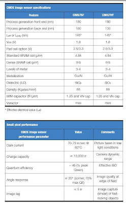
After the recent wave of layoffs IBM image sensor business is probably not in best shape. Still, IBM CIS process brochure contains interesting process data:

IBM CIMG7SF and CIMG7HY offer 4T reference pixel with an optimized transfer gate. CIMG7SF uses a full 180nm technology and provides clients with a 5.0um reference pixel for design, as well as support for custom pixel designs. This technology is ideal for high-end applications and also supports reticle stitching for large die applications.

CIMG7HY uses 130nm technology for the metal layers to achieve reduced wiring pitches in the pixel array. This technology is ideal for small-format applications and provides the client with a 2.0 and 2.2um reference pixel using a 4T 4-shared (4T/4S) architecture. CIMG7HY also provides support for sub-2.0um custom pixel designs.

Both CIMG7SF and CIMG7HY include microlenses and color filters, along with pinned photodiode technology for reduced dark current. CIMG uses aluminum wiring for the last metal level and copper (Cu) wiring for the remaining metal levels. With thin back-end-of-line (BEOL) metal stacks and improved dielectric tolerance, CIMG is ideal for all your imaging needs.


Update: IBM put another image sensor brochure on-line. It mentions that IBM offers reticle stitching for large area sensors and also gives the pixel cross-section:

Sunday, August 17, 2008

Sony Announced PAL/NTSC CCDs for Security

Sony Cx-News magazine has announcement of 4 new CCDs for security cameras. Sony incrementally reduced the stack hight and changed complementary color filters, resulting in 7db sensitivity improvement. Also, the new CCDs can work with 3.3V for the horizontal clocks and the reset clock.

Friday, August 15, 2008

Taiwan Notebook OEMs Want to Design Image Sensors In-House

Digitimes: Leading notebook OEMs in Taiwan, including Quanta Computer, are said to be growing their in-house CMOS image sensor development, according to Digitimes sources at CMOS image sensor vendors. As built-in webcams are gaining penetration in notebooks, some OEMs have considered increasing their own CMOS image sensor development to cut costs, the sources explained.

Quanta responded that it will not strategically devote specialized efforts on CMOS image sensor development, and is still placing component orders in accordance to bookings.

Thursday, August 14, 2008

Omnivision Loses Customers

Barron's: Robert W. Baird analyst Tristan Gerra says that his checks in Asia find OmniVision “should lose most sockets at a key tier-one mobile phone OEM” in the second half of the year. He also reports that competition in the VGA sensor market is worsening, with ASPs as low as 60 cents.

“We see no catalyst for OVTI shares near-term as the normally seasonally strong October quarter should experience muted growth this year, followed by two seasonally weak quarters,” he writes.

Gerra also notes that Aptina is regaining share in both mobile phones and notebooks.

Update: Business Week adds that Gerra believes 3MP no longer represents a meaningful revenue catalyst for the company this year. Reuters quotes Robert W. Baird saying that the Chinese mobile phone market has further slowed down in July and August following initial weakness in the second quarter, hurting Omnivision's VGA sensor demand.

Pixart to Supply VGA Sensors for Asus Eee

Digitimes: Pixart has landed orders for about 200,000 VGA CMOS image sensors for Asus Eee notebook.

Wednesday, August 13, 2008

TSMC Expands 0.11um CIS Capacity

Digitimes, EETimes: TSMC board approved US$107.4M capex to upgrade a portion of 0.18um logic process capacity to 0.11um CMOS image sensor and other advanced processes.

Tuesday, August 12, 2008

InfoTrends Predicts 1.3B Camera Phones Sold in 2012

According to a new report from InfoTrends entitled Worldwide Camera Phone Forecast: 2007-2012, worldwide shipments of camera phones will jump from over 700 million units in 2007 to surpass 1.3 billion in 2012. This growth will be driven largely by the Asia-Pacific and ROW regions, where revenues will increase at respective CAGRs of 15% and 24%.

Siimpel AF Appears in Motorola Phone

Yahoo: Siimpel announced that it’s AF SF9x MEMS-based silicon camera technology is now shipping in Motorola’s recently announced MING A1600 cellular handset, which integrates the industry’s first MEMS-based, continuous autofocus camera.

Saturday, August 09, 2008

Image Sensor Companies in China

With all eyes on Beijing these days, I decided to put together few words about our colleagues in China.

In 2001 Nanjing Micro One Electronics introduced the first homemade CMOS image sensor in China. However, due to low demand for CMOS image sensors in China and competition from the image sensor market leaders, such as Omnivision, Micro One subsequently withdrew from this market. Today there are 3 companies designing image sensors in mainland China: Superpix, Galaxycore and Rui Xin Microelectronics.

Galaxycore is the oldest one, founded in 2003 and is based in Shanghai.

SuperPix Micro Technology (SPMT) was founded in 2004 and is based in Beijing. In 2006 it brought the first Chinese 2MP chip to the market, reportedly manufactured by Tower.

KunShan RuiXin Microelectronics is the most recent upstart, founded in 2006 by former employees of SMIC and DALSA. Now it's group of 35 engineers, designed 6 sensors.

Thanks to O-A for the information.

Friday, August 08, 2008

Pixart to Launch Webcam SoC in 2009

Digitimes: Pixart says that it will launch a web camera SoC composed of a ISP and sensor in the Q1 2009. Since most rivals still have designs where the ISP and sensor are separate, and customer feedback to the SoC has been good, Pixart is confident about the solution's performance.

With Nintendo sales flat, webcam sensors are expected to be the company's key sales driver in the Q3 2008 with a sales contribution of about 10%. Strong growth is expected to maintain throughout the coming two years.

Thursday, August 07, 2008

Nanotechnology in Image Sensors #2

Electronics Web: Scientists at the U.S. Department of Energy's Lawrence Berkeley National Laboratory and the University of California at Berkeley have created all-integrated sensor circuit based on nanowire arrays, combining light sensors and electronics made of different crystalline materials.

For their integrated nanowire photosensor circuitry, Ali Javey group in Berkeley Lab's Materials Sciences Division used cadmium selenide nanowires as visible-light sensors. For the electronics, nanowires with a germanium core and a silicon shell were the basis of field-effect transistors that would amplify the current produced by the photosensors in response to light by five orders of magnitude.

The nanowires density is not that remarkable comparing with the modern 65-90nm CMOS processes:


About 80% of pixels are connected - impressive, considering the simple technology used.

Nanotechnology in Image Sensors #1

Medgadget, BBC, Reuters: Scientists at Northwestern University and University of Illinois at Urbana-Champaign have developed technology that allows for building curved sensors and accompanying electronics. It relies upon an array of pixels interconnected by small wires. Using a flexible, temporary backing, the researchers can form the array into a curved shape. While a flat, planar sensor cannot flex without damaging its light-sensitive pixels, the new technology puts the strain on the wires, each flexing as much as 40 percent. Since the wires absorb the strain, the pixels are barely stressed, even when affixed to the retina-shaped housing of the new experimental camera.

Tuesday, August 05, 2008

ST On Image Sensor Challenges

Jean-Luc Jaffard from ST imaging Division delivered a good image sensor presentation on Design Automation and Test in Europe Conference (DATE'08). Some interesting parts from the presentation:
  1. Due to ever increasing number of special process tweaks in modern sensor manufacturing, "CMOS Process with Imager Options" migrates towards "Imager Process, CMOS Capable".

  2. ST is going to use 12" Cu wafers for 1.4um pixel production.

  3. 3D sensor-analog front end integration gives only 30% of full well increase for 1.4um pixels, despite the added process complexity and cost.

  4. Same BW BSI images and graphs appear. I wonder why ST does not show its color results. It's hard to support claims on BSI superiority without bayer-patterned sensor QE graphs.

Noise Primer by Eric Fossum

Eric Fossum posted a nice 4T pixel noise explanation on dpreview forum:

"In an active pixel sensor with intra pixel charge transfer, the photodetector is pretty much decoupled from the floating diffusion and SF amplifier. The latter's sizing is usually determined by design rule (e.g. 0.25 um or lower) whereas the former is determined by sensor physical size and resolution, unless it is for camera phones in which case the photodetector is made as small as possible yet still have decent QE, full well, etc.

So, true, gain in the SF is inversely proportional to the FD capacitance which in turn scales like the area of the SF gate and FD node, and parasitics, and sometimes intentional capacitance.

In this amplifier, the kTC noise is mostly removed by correlated double sampling. In theory, totally removed, but only if the sampling is perfect and the SF transistor itself has no noise. In fact, that transistor does have several noise sources. The dominant one these days is the so called 1/f noise. Actually, it is only loosely 1/f. The noise is believed to come from fluctuations in the carrier density under the gate. As carriers get trapped at the Si-SiO2 interface (or within a short distance thereof) they partially screen the gate field and change the electrostatics of the structure. The resultant change in semiconductor carrier density results in a change in current. The trapped carriers dont stay trapped forever. It depends on the trap energy and the distance of the trap from the Si SiO2 interface with lots of time and temperature dependencies. So, carriers get trapped, carriers get released, and the current thru the source-follower fluctuates "randomly" in time. If you are lucky enough you can see the effect of a single trap being filled and emptied as the current fluctuates between 2 different levels (small fluctuation mind you). This is the "random telegraph signal" or RTS noise. The ensemble of traps can lead to 1/f like behavior in the spectrum of the noise.

Actually, trap densities are of the order of 10^10 per cm^2. So, a gate that is, say, 0.25 um long and 1.0 um wide is 0.25x10^-8 cm^2 and contains a handful of traps, on average. So, it is easy to see that some transistors may be more noisy than others depending on the number and type of trap present.

The effect of these traps increases as the gate area decreases and 1/f noise increases with smaller transistors. So, to the extent smaller pixels have smaller transistors (not necessarily true, of course) then smaller pixels would be noisier than larger pixels.

This depends on how you measure the noise. I have been referring to fluctuations in current around some nominal operating point, relative to the nominal current. If you measure the current fluctuation as an effective gate voltage change, and then relate that via capacitance to an effective number of electrons, the read noise could go up or down or stay constant. It depends on how the other things scale. You could also measure noise in input-referred electrons as a fraction of full well, in electrons. This would then bring the photodetector into play if the full well was limited by the detector. The full well could also be clipped by a combination of low sense node capacitance (FD) and low voltage swing (amplifier limited full well). Usually the design tries to match these things.

1/f noise also depends on the process, and design, and also biasing. It is generally lower for p-channel devices compared to n-channel, but then to get teh same current drive, the p-channel has to be larger since the hole mobility is like half that of the electron mobility. Buried channel transistors have lower 1/f noise than surface channel but have higher operating voltage requirements or have lower swing for the same operating voltage. Many tradeoffs are available to the designer. Also, these things evolve in time esp. once they become limiting factors. Nothing like hundreds of engineers trying to fix a problem.

So, combing the literature and comparing noise and pixel size is not going to give you definitive answers. It is hard to get consistent results in your own fab doing your own test chips from run to run. Apparently the phase of the moon and sunspot count, and butterfy activity in South America all count.
What was the question? Oh yes, what can be expected.

Sub electron read noise has already been demonstrated in rare cases, and a few electrons in several cases. Low read noise is not so important is DSLRs because most photographers are going to be limited by shot noise or something else rather than read noise. However, for light-starved small pixels in camera phones that people want to use in poorly lit bars, low light is a persistent problem and low read noise is always desired."

Monday, August 04, 2008

Recent BSI Developments Review

Semiconductor International published a nice review of recent developments in consumer BSI sensors. It covers pretty much all the recent news from Omnivision-TSMC, ST, Sony, Sarnoff and others.

Friday, August 01, 2008

Pixelplus Announces 1.75um Pixels

Pixelplus quietly put 1.75um pixel announcement on its web site:

"Pixelplus introduces most advanced 1/4" 3.0M bayer CMOS Image Sensor, PS2320, with the highest pixel performance of 1.75 x 1.75 um2 size. The PS2320 has the highest figure of merit both in performance and economics. The PS2320 can save power consumption, module size as well as module height which can satisfy who want to build high performance, high resolution and much slim-look application."

While being 2 years behind the leaders with 1.75um generation, Pixelplus is still ahead of Magnachip, Siliconfile and few other smaller companies - not a bad result. I just wonder where is the official PR on this achievement.

Kodak Increases CIS Investment

Seeking Alpha publishes Kodak Q2'08 Earnings Call transcript. Antonio Perez, the CEO, says that Kodak has increased investment in CMOS image sensors. He also updates on 1.4um pixel progress:

"We continue to believe in the potential of our CMOS technology and the market opportunity it offers. Next year, we expect to be in production with the industry’s first one-quarter-inch, 1.4 micron 5 megapixel sensor, which is a leap ahead in image quality."