Discovery: Florida University research group under Franky So lead describes a new night vision technology in a recent article in the journal Advanced Materials that was funded in part by DARPA.
Infrared light enters the film and is detected by the first of seven separate layers, which generates a slight electrical charge. Additional electrical energy -- about three to five volts -- amplifies that signal, which is then converted back into visible light.
Like most of today's night vision cameras, So's device emits an eerie green light. Unlike most night vision technology today, however, So's design would weigh less than 100 grams. Part of that weight is the proof of concept small size -- about one square centimeter -- but So says that even a full scale device could weigh as little as 10 grams and be only a few microns thick.
It will take about 18 months to scale up the device for practical applications, such as car windshields, lightweight night vision eyeglasses and cell phones cameras.
University Florida page adds some details about the new technology. All organic up-conversion devices are realized by integrating an OLED and an organic photodetector into one device. Prior art NIR-to-visible light up-conversion devices, integrating an inorganic LED with an inorganic photodetector, have been reported but the maximum external conversion efficiency was about 0.3%. Organic version is supposed to have an advantage in this.
Thanks to A.A. for sending me the link.
Thursday, April 29, 2010
Tessera Got First EDoF Royalties
Business Wire: Tessera announced its Q1 2010 results. Imaging & Optics revenue was comprised of $3.1M in royalties and license fees, and $5.4M in products and services. Tessera siaid it received first royalties for its EDOF technology in the first quarter. The company anticipates EDOF royalties will continue to grow throughout this year as additional OEMs ship mobile camera modules with our EDOF technology.
In terms of outlook, Q2 2010 Imaging & Optics royalties and license fees revenue is expected to range between $3.0 M to $3.5M. Imaging & Optics products and services revenue is expected to range between $5.5M to $6.0M.
In terms of outlook, Q2 2010 Imaging & Optics royalties and license fees revenue is expected to range between $3.0 M to $3.5M. Imaging & Optics products and services revenue is expected to range between $5.5M to $6.0M.
Wednesday, April 28, 2010
TSMC Working on 1.19um Pixel?
Seeking Alpha TSMC Q1 2010 Earnings Call transcript mentions new pixel development activity:
Shang-Yi Chiang, SVP, R&D:
"We are working with customers on 1.19 micron pixel, and TSMC is the first one to introduce this thing called BSI technology, backside illumination. There are certain advantages if we shine light from the backside, and in this case we had to slim down the wafer to 3 microns thick. The handling, the technology, extremely difficult. We already shipped products using this BSI technology in 8-inch wafers and we are working on 12-inch wafers right now."
Omnivision reported earlier that it's working on 1.1um pixel. So, who is this customer designing 1.19um pixels? Shang-Yi used to be Visera chairman for 3 years or so, it's hard to believe that he made a mistake with pixel size.
Nokia N8 Features "The Biggest Sensor In A Mobile Device"
Nokia Conversations published a conversation with Damian Dinning, Nokia’s main man for imaging describing the camera portion of the newly announced 12MP N8 camera phone. The official HW spec for the phone does not tell the sensor size, while Damian says it's "the biggest sensor in a mobile device". One of the tweets seemingly belonging to Nokia insider reports that the sensor size is 1/2-inch. GSMArena claims the sensor size is 1/1.9-inch without disclosing its sources. These numbers translate into about 1.6-1.7um pixel size.
Nokia Conversations writes:
"The team behind the Nokia N8’s camera want to set new benchmarks. Not just for the quality of the still image camera, but the video recording as well. Across both uses, the team have been optimising each specific element of the device’s camera for as many use cases as possible. Cracking Improving the low light performance nut is one of the hardest challenges for mobile device cameras. Naturally, that’s where the camera team started. This time though, the effort was focussed not just on still images, but on video too.
In dramatically improving low light performance, the team were able to improve performance in bright conditions as well."
N8 records 720p/25fps HD video. The images it produces (both still and moving) are said to "sport a surprisingly high degree of detail, but without any much of the noise you see in images from some other devices". The sample pictures and video seem to confirm that.
The phone is expected to go on sale in Q3, 2010.
Sunday, April 25, 2010
2010 Vertically Integrated Pixel Sensors Workshop Materials On-Line
Electrons and Holes blog posted the link to the materials presented at Workshop on Vertically Integrated Pixel Sensors - VIPS 2010, held on April 22-24, 2010 in Pavia, Italy. While the workshop mostly concentrates of radiation and particle detectors, it has few presentations showing interesting current and future works coming from 3D integration:
IMEC slides show 3D integration roadmap:
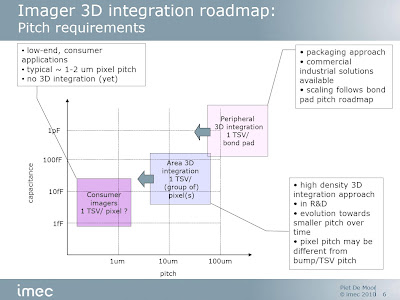
If/when 1 TSV per group of pixels approach is adapted, it would completely redefine the speed and noise trade-offs in the future sensors. The image processing pipeline might be lagging though.
Another slide presents IMEC work on crosstalk reduction in BSI sensors:

Yet another IMEC slide talks about backside passivation trade-offs:

Fraunhofer Instutute together with Berlin University presented quite impressive photos of wafer-level cameras:

ST too presented its WLC packaging and process:

Saturday, April 24, 2010
Teradyne Sees No Image Sensors Recovery
Seeking Alpha: Teradyne Q1 2010 Earnings call has few words about image sensor tester sales still being slow. Basically, Teradyne does not believe it loses market share on sensor testers market. Rather, it says that the market has not recovered yet.
Qualtre Promises to Solve Gyro's Slow Drift Problem
PR Newswire, EETimes: Qualtre is developing a solid-state multi-axis MEMS gyroscopes digital camera image stabilization, among other things. Commercially available MEMS gyroscopes serving these applications have delicate moving mass structures vibrating at low frequencies of 5-50KHz, making them susceptible to bias drift over time, temperature and vibration. Qualtre gyroscopes operate at high frequency (2-10MHz) bulk acoustic modes to provide superior mechanical signal amplification with excellent bias stability over an extended temperature range.
If Qualtre really delivers a product with greatly reduced drift over time, it would be a major improvement in long exposure image stabilization. So far the gyro's slow drift is the main reason that still image stabilization is less than perfect at 1-2s exposures.
Founded in 2008, Qualtre is a venture-backed company founded by Dr. Farrokh Ayazi from Georgia Tech's Integrated MEMS Laboratory. The company just announced that it has completed an $8M Series B round of financing, bringing the total funds raised to $13M. Matrix Partners and Pilot House Ventures participated both A and B investment rounds with no new investor joined.
Friday, April 23, 2010
Toshiba To Boost CMOS Image Sensor Output By 20%
Nikkei Business News: Toshiba plans to increase production of its CMOS sensors by 20% during the April-September half.
The access to full article is restricted to subscribers only. It would be great if somebody with the full access can provide more details on this.
The access to full article is restricted to subscribers only. It would be great if somebody with the full access can provide more details on this.
Webcast on CMOS Image Sensors Technologies & Markets
Yole Développement to hold webcast on CMOS image sensors technologies & markets on May 6, 2010. Thanks to R.F. for sending me the link.
IMEC Demos Video Fusion
Repost from Electrons and Holes blog: At 2010 NAB Show IMEC announced "virtual camera" merging few HD video streams into a one where a viewpoint can be smoothly changed. Now IMEC published a Youtube video showing the system's amazing capabilities:
100Mfps-fast Averaging CCD Paper
Free-access Sensors Journal published a paper proposing a very fast CCD sensor. The proposed CCD uses in-pixel 100-200 memory storage cells to achieve up to 100Mfps speed and is able to accumulate the signal to improve SNR:
Etoh, Takeharu Goji; Son, Dao Vu Truong; Akino, Toshiaki Koike; Akino, Toshiro; Nishi, Kenji; Kureta, Masatoshi; Arai, Masatoshi. 2010. "Ultra-High-Speed Image Signal Accumulation Sensor." Sensors 10, no. 4: 4100-4113.
(via Electrones and Holes blog)
Etoh, Takeharu Goji; Son, Dao Vu Truong; Akino, Toshiaki Koike; Akino, Toshiro; Nishi, Kenji; Kureta, Masatoshi; Arai, Masatoshi. 2010. "Ultra-High-Speed Image Signal Accumulation Sensor." Sensors 10, no. 4: 4100-4113.
(via Electrones and Holes blog)
Peter Denyer Passed Away
Peter Denyer, the founder of VVL in Edinburgh, and now part of ST Microelectronics, passed away yesterday.
From University of Edinburgh page: By the early 1980s the research team, lead by Prof. John Mavor and then Prof. Peter Denyer gained an international reputation for first CCD and then MOS analogue and digital IC design with special application to signal processing. In 1986 Peter Denyer was appointed as the University’s then youngest Professor to a position sponsored by Advent, a leading Venture Capital house.
In 1989 Renshaw, Denyer, Wang and Lu published a paper reporting work started in 1986 on CMOS image sensing that culminated in the design and demonstration of the world's fist single chip CMOS video camera.
In 1990, with University and Venture Capital backing, Denyer and Renshaw set up VLSI Vision (VVL) a University Spin out company, to sell the single chip video camera device and develop a family of novel imaging devices based on this technology. This company grew from one employee to over 100 in the five years to 1995, when it became the first spin out company from a Scottish University to become a PLC, placed on the London Stock Exchange. Peter was the CEO of VISION Group plc, a company he founded, took to IPO and to profitability over a 9-year period from 1990 to 1999.
By 1995 competition started from other new companies based in the US and far east. To address the emerging market and cope with the competition, VVL sought to expand its operation and as a consequence was taken over in 1999 by ST Microelectronics, to form a new Imaging Division of that company, to address the newly emerging mass market in mobile phone cameras.
Since the sale of VISION Peter has become an active angel investor, founding five new businesses, and leading two further IPOs.
Namely, Peter co-founded and chaired Microemissive Displays (MED), the world’s leading developer of polymer organic light emitting diode (P-OLED)-based microdisplays which floated on AIM in November 2004 and he co-founded and Chaired Rhetorical Group plc, a leading speech synthesis company, which was sold to Scansoft Inc. in 2005. He served as a director of MED and also chaired another technology company Eleksen Ltd which develops technology and applications for sensing fabric. Peter also served as chairman of Quantum Filament Technology commercializing a novel field emission approach for the next generation of flat displays. Peter was a Director and Non-Executive Chairman of Dexela Limited designing large-area X-ray sensors for mammography.
For his work on the technology and its commercialization, Peter received the Royal Academy of Engineering Silver Medal, the IEEE Millennium Award, and the Queen’s Award for Technology (link).
This sad news was brought to me by A.T.
Update: Peter's funeral is on Thursday 29th April at 2pm at the Main Chapel at Mortonhall Crematorium in Edinburgh.
PTC Series Continues
Albert Theuwissen continues his educational series on PTC as the most informative tool telling about image sensor performance. The recent article integrates all the noise sources in the dark.
2011 International Image Sensor Workshop Time and Location Posted
2011 International Image Sensor Workshop (IISW) time and location has been posted on www.imagesensors.org. It's Ōnuma Quasi-National Park, Hokkaido, Japan on June 8-11, 2011.
Thanks to E.F. for letting me know.
Thanks to E.F. for letting me know.
e2v Supplies CCD for NASA Solar Mission
Electronics Weekly reports that e2v CCDs are used in NASA Solar Dynamics Observatory (SDO) project.
Thursday, April 22, 2010
LensVector to Support U.S. Intelligence Missions
Business Wire, Cnet: LensVector announced a strategic investment and development agreement with IQT, the independent strategic investment firm that identifies innovative technology solutions to support the missions of the CIA and other U.S. Intelligence organizations. “LensVector’s solid-state optics technology provides a novel foundational capability that is crucial to the missions of many government agencies,” said William Strecker, EVP of Architecture and Engineering and CTO at IQT.
Wednesday, April 21, 2010
Nokia's EVP Predicts Camera-Phones to Make SLR Cameras Obsolete
Reuters, The Register: Fast developing cameraphone technology will shortly make SLR system cameras and even professional cameras obsolete, Nokia's Markets EVP Anssi Vanjoki said in a speech in Helsinki.
"There will be no need to carry around those heavy lenses," Vanjoki said, pointing to a professional photographer taking pictures of him.
Vanjoki said HD video recording was also coming to cellphones within the next 12 months.
"There will be no need to carry around those heavy lenses," Vanjoki said, pointing to a professional photographer taking pictures of him.
Vanjoki said HD video recording was also coming to cellphones within the next 12 months.
Omnivision Announces 720p HDR Sensor
PR Newswire: Omnivision announced a new flagship SoC sensor for security - the OV10630. The new sensor combines 720p/30fps HD video with color HDR full image processing pipeline in a 1/2.7 inch optical format. OV10630 delivers 110dB dynamic range in black-and-white and 100dB + in color.
The OV10630 design is based on a 4.2um OmniPixel3-HS pixel having "unparalleled low-light sensitivity". The OV10630 has an active array of 1280 x 800 pixels. The image pipeline has also all required automatic image control functions, including automatic exposure control, automatic white balance, automatic black level calibration, as well as defective pixel correction, gamma correction and lens shading correction.
The OV10630 is now sampling, and is scheduled to enter mass production by the fourth quarter of 2010.
Tuesday, April 20, 2010
Next iPhone Might Have Dual Camera
It looks like Gizmodo was able to get a hold on the next generation iPhone prototype. The prototype has has dual camera - a small one is front-facing and a bigger one is on the back.
Thanks to R.C. for the link.
Update: Korean Chosun Ilbo reports that LG Innotek is supplying the camera module for iPhone 4G. The camera modules are manufactured at its plant in Gumi since April 2010. The company will mass produce them starting in the second half of this year.
Thanks to R.C. for the link.
Update: Korean Chosun Ilbo reports that LG Innotek is supplying the camera module for iPhone 4G. The camera modules are manufactured at its plant in Gumi since April 2010. The company will mass produce them starting in the second half of this year.
Saturday, April 17, 2010
Semiconductor International is No More
Semiconductor International is shutting down. Its web site will close on April 30, 2010. Those who'd like to keep its nice image sensor-related articles have little time to save them in private place. Some recent interesting articles are:
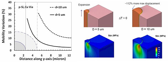
Philip Garrou series on 3D packaging, including the recent article on 3D integration stress management talking about larger-diameter TSVs causing large mobility changes in silicon because of large deformation and shear stress. (Source: Synopsys):

Alother Philip's article talks about the recent trends in TSV technology and packaging. Generally, The 3D panel on IMAPS 2007 conference was in complete agreement that the 3D IC market has evolved into two main segments:

Prismark revealed their 2014 market projection of 3.2M TSV wafers consisting of
Application 3-D % of Appl
Image Sensors 90
Rf/SiP 15
MEMS 20
Logic <1
DRAM 7
Other memory 1
Semiconductor International used to be a place where Chipworks' Dick James published many reverse engineering findings, such as this one: DSLR Image Sensor Innovation – Who Is Challenging Canon and Nikon’s lead?, from September 11, 2009.
It's a pity that this wealth of information is going to disappear by the end of this month.
Philip Garrou series on 3D packaging, including the recent article on 3D integration stress management talking about larger-diameter TSVs causing large mobility changes in silicon because of large deformation and shear stress. (Source: Synopsys):
Alother Philip's article talks about the recent trends in TSV technology and packaging. Generally, The 3D panel on IMAPS 2007 conference was in complete agreement that the 3D IC market has evolved into two main segments:
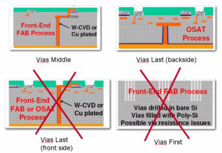
- (1) vias middle either Cu or W and
- (2) vias last from backside Cu (see below)
- Anything else will be niche.
Prismark revealed their 2014 market projection of 3.2M TSV wafers consisting of
Application 3-D % of Appl
Image Sensors 90
Rf/SiP 15
MEMS 20
Logic <1
DRAM 7
Other memory 1
Semiconductor International used to be a place where Chipworks' Dick James published many reverse engineering findings, such as this one: DSLR Image Sensor Innovation – Who Is Challenging Canon and Nikon’s lead?, from September 11, 2009.
It's a pity that this wealth of information is going to disappear by the end of this month.
Friday, April 16, 2010
NIST Detector Counts Photons With 99% QE
Detecting single photons with confidence is not easy: National Institute of Standards and Technology (NIST) has developed "the world’s most efficient single photon detector", which is able to count individual photons with roughly 99 percent efficiency. The basic principle of the detector is to use a superconductor as an ultra-sensitive thermometer. Each individual photon hitting the detector raises the temperature—and increases electrical resistance—by a minute amount, which the instrument registers as the presence of a photon.
“When these detectors indicate they’ve spotted a photon, they’re trustworthy. They don’t give false positives,” says Sae Woo Nam, a physicist with NIST’s Optoelectronics division. “Other types of detectors have really high gain so they can measure a single photon, but their noise levels are such that occasionally a noise glitch is mistakenly identified as a photon. This causes an error in the measurement. Reducing these errors is really important for those who are doing calculations or communications.”
“We can’t be sure from direct measurement that we’ve achieved 99 percent efficiency because the metrology is not in place to determine how close we are—there’s no well-established technique,” Nam says. “What is great about our latest progress is that we measure nearly the same detection efficiency for every device we build, package and test. It’s the reproducibility that gives us confidence.”
The work was presented at the SPIE Symposium on Defense, Security, and Sensing in Orlando World Center Marriott Resort and Convention Center on April 7, 2010: A.E. Lita, B. Calkins, L.A. Pellouchoud, A.J. Miller and S. Nam. Superconducting transition-edge sensors optimized for high-efficiency photon-number resolving detectors.
Wednesday, April 14, 2010
Aptina, Omnivision Narrowly Missed Golden Mousetrap Award
Business Wire: Aptina MT9M033 HDR image sensor has been named a finalist in the Design News Golden Mousetrap Best Products contest. For more than two decades, Design News has recognized engineering innovation and creativity in product design. “These products, as always, showcase the highly imaginative ways that today's engineers are ‘building a better mousetrap,’ and we thank them for their contributions,” said Jennifer Roy, Managing Editor for Design News.
Unfortunately, MT9M033 did not win the Award this year. For that matter, no other image sensor won, although Finalists list has two of them: Aptina MT9M033 and Omnivision Cameracube.
Unfortunately, MT9M033 did not win the Award this year. For that matter, no other image sensor won, although Finalists list has two of them: Aptina MT9M033 and Omnivision Cameracube.
Omnivision is Declared #1 on Camera Phone Market
Investors Business Daily published article composed of quotes from different analysts on Omnivision:
"We believe they're going to be in the new-generation iPhone, which will generate momentum in the second half of the calendar year," said Tristan Gerra, a senior analyst at Robert W. Baird & Co. "We're seeing a sharp pickup in smart phone orders right now," Gerra said. "This certainly helps Omni, given that it's the No. 1 supplier of image sensors in the cell phone market."
"The prospect of Verizon possibly carrying the iPhone has driven a lot of the excitement behind OmniVision's stock," said Betsy Van Hees, an analyst at Wedbush. "OmniVision is a product cycle story. The big growth driver is the fact that we're seeing smart phones move from three to five megapixels."
Raymond James analyst Hans Mosesmann expresses "concerns on mega-pixel density stagnation with a market that may not wish to pay the premium OmniVision's best-in-class technology delivers."

Tuesday, April 13, 2010
Aptina Adopts Apache's Noise and Power CAD Tools
Business Wire: Aptina has adopted Apache’s RedHawk-NX and Totem-MMX tools. Aptina will use Apache’s Totem-MMX, a transistor-level power / ground noise analysis and verification solution, to analyze and sign-off the huge analog sensor arrays which are implemented using custom-layout of transistors. The image sensor array is then compiled into accurate and efficient custom macro model (CMM) and imported to RedHawk-NX for a full-chip, mixed-signal dynamic power integrity simulation. The combination of Totem and RedHawk allows Aptina to consider the impact of analog transient supply currents on the digital logic of the SoC. Apache’s high-capacity integrated solution helps prevent power-related design failures.
Apple to Use Sony Sensors in 2011 iPhone?
TheStreet quotes Rodman Renshaw analyst Ashok Kumar saying that Apple has picked Sony's 8MP sensor for the 2011 iPhone. The move would displace OmniVision, Apple's current camera supplier to the iPhone. Since last year, OmniVision has been Apple's exclusive camera chip supplier to the iPhone. OmniVision is expected to supply a 5MP camera for the upcoming version of the iPhone due out this summer, said Kumar.
MacRumors notes that Kumar carries a mixed record in his previous predictions.
MacRumors notes that Kumar carries a mixed record in his previous predictions.
Friday, April 09, 2010
Rolling Shutter Reduction in Video
PrMac: While not directly related to image sensors, Australian company CoreMelt presents rolling shutter reduction extension to it's video image stabilization software. Quite an obvious idea when one thinks about it, but CoreMelt claims its the only video stabilization software with rolling shutter reduction. CoreMelt demos its software at NAB 2010.
However, just a year ago at NAB 2009 another company, UK-based The Foundry, presented its own rolling shutter reduction subroutine.
With modern power ISPs and gyros embedded in every other camera phone, one can guess that sooner or later rolling shutter compensation becomes a standard ISP feature.
There are some extreme cases of the rolling shutter wobbling on Youtube. A good compensation subroutine has to deal with cases like this one:
Thursday, April 08, 2010
Samsung 1.75um Sensors Feature EDoF, 70Lux SNR10
Business Wire: Samsung announced two new image sensors – 1.3MP S5K6A1 and 2.1MP S5K5B3 - for use in notebook computers and other devices requiring video capture. Using 1.75um pixels, the new imagers are said to have significantly improved low light sensitivity of 70Lux of YSNR10.
The 2.1MP S5K5B3 has an embedded EDoF to allow bar codes and business card reading without needing mechanical AF support. In February Tessera reported that Samsung is its EDoF licensee. S5K5B3 sensor supports camera modules with full 1080p HD at 30fps capability in a z-height less than 4.5mm. S5K6A1 sensor has been designed for camera modules with 720p HD at 30fps capability in a z-height less than 3.5mm.
Samples for both of these image sensors are currently available with mass production scheduled for Q2 2010.
According to TSR, the notebook and PC camera market is expected to reach 150M units in 2010 and grow at a compound annual growth rate of 12% to reach 200M units by 2013. The camera attachment rate of over 70% now, according to Dojun Rhee, VP of System LSI marketing, Samsung Electronics.
Wednesday, April 07, 2010
Fast Sensors Standoff
Photron and Vision Research announced new fast cameras toward 2010 NAB Show in Las Vegas. Both use custom designed sensors
Business Wire: Photron Fastcam BC2 delivers 1000fps at its native 4MP resolution 2048x2048 or up to 2000fps at 1920x1080 HD resolution (no word "progressive" though). The camera appears to be a broadcaster's version of Fastcam SA2 announced a year ago, I believe.
Marketwire: Vision Research announced Phantom Flex featuring 4MP CMOS sensor with resolution of 2560x1600. When set to Standard Mode the maximum recording speed of 1,560fps at 4MP resolution. In full-HD resolution (1920x1080), the Phantom Flex offers a maximum recording speed of 2,800fps. When reduced to 720p HD resolution (1280x720), the Phantom Flex offers a maximum recording speed of 6,100fps. The camera can go even faster, recording at 13,000 fps at 640x480, also in Standard Mode.
Other than Standard, there is also HQ Mode, where the Vision Research's Flex trades speed for enhanced image quality; the camera still offers impressive maximum recording speeds of 780 fps at 2560x1600, 1,390 fps at 1920x1080, and 3,000 fps at 1280x720 resolutions. HQ Mode is said to employ a proprietary multi-sampling image enhancement technology to deliver stable blacks, low noise, higher dynamic range and repeatable shots over the full range of supported resolutions, frame rates, and temperatures.
PTC with All Noises Integrated
Albert Theuwissen published another post on PTC curve with all kind of noises integrated into PTC graphs. Then the post explains how to extract fixed pattern-like parameters from the PTC measurements. Next post will talk about temporal noise data extraction.
Canesta Features in NY Times
As Electrons and Holes blog mentions, NY Times has an article on Canesta 11-year history. The article is accompanied by two video demos showing gaiming and TV remote control applications.
Over the years, Canesta has raised about $60M. Quanta and Honda are among the investors. Quanta expects to sell laptops with 3D camera later this year. Canesta hopes to piggyback on the exploding interest in the technology and pop low-cost chips into every device it can.
Over the years, Canesta has raised about $60M. Quanta and Honda are among the investors. Quanta expects to sell laptops with 3D camera later this year. Canesta hopes to piggyback on the exploding interest in the technology and pop low-cost chips into every device it can.
Tuesday, April 06, 2010
Silecs Polymer Lightpipes
Finnish company Silecs together with IBM presented high refractive index siloxane polymer lightguide at IISW 2009. Now the detailed study is published in the form of MS Thesis at Aalto University: "Spin-on siloxane polymers in image sensor applications" by Kimmo Karaste. A clear QE enhancement has been shown, unfortunately, accompanied by a crosstalk degradation (2.2um IBM pixels):

Also, the earlier ML AR coating results are presented (based on Tower 2.8um pixels).

Also, the earlier ML AR coating results are presented (based on Tower 2.8um pixels).
Panasonic Image Sensor Roadmap
Panasonic published March 2010 edition of its DSC image sensor roadmap:

Comparing this roadmap with its previous version from March 2009, 16MP and 18MP products are moved much farther in future. Instead, the high sensitivity I and II products are added.
Similarly, security, broadcast and industrial-targeted roadmap abandons high resolution sensors. Instead it's emphasizing transition form CCD to MOS sensors. The first figure is from March 2010, the next one is from a year earlier.


Monday, April 05, 2010
Historical View on Image Sensor Market
EETimes has an interesting article about semiconductor industry ever-changing leadership by Walden Rhines, Mentor Graphics CEO. It has an interesting passage about image sensor market:
"One of the more amazing aspects of the increasing pervasion of semiconductors into new applications is the significant growth in revenue of existing applications as the cost per unit decreases. Consider the digital camera. Most of the semiconductor content of a digital camera consists of non-volatile FLASH memory and the image sensor. In the early 1990s, solid state image sensors sold for $20-25. Image sensors were a negligible portion of the semiconductor total available market (TAM) until the current decade. During the 1990s the price per sensor fell dramatically from the $20-25 range to about $5. At this price point, unit volume soared, making image sensors more than 3 percent of the semiconductor TAM in the last few years. ...The result was a substantial net growth in the market for digital cameras and the semiconductors required to make them."

"One of the more amazing aspects of the increasing pervasion of semiconductors into new applications is the significant growth in revenue of existing applications as the cost per unit decreases. Consider the digital camera. Most of the semiconductor content of a digital camera consists of non-volatile FLASH memory and the image sensor. In the early 1990s, solid state image sensors sold for $20-25. Image sensors were a negligible portion of the semiconductor total available market (TAM) until the current decade. During the 1990s the price per sensor fell dramatically from the $20-25 range to about $5. At this price point, unit volume soared, making image sensors more than 3 percent of the semiconductor TAM in the last few years. ...The result was a substantial net growth in the market for digital cameras and the semiconductors required to make them."

Kodak Announced Aromatography - An Unbelievable Sensory Experience
Another April Fools announcement came from Kodak. Thanks to recent breakthroughs in Neuro-Optic-Nasal-Sense Imaging Kodak found a way of transferring delicate and complex aromas that accompany the visual experience. New imaging sensors and software developed by Kodak have made the dream into a reality. Dr. Harold Museau, PhD. , inventor of Aromatography, graciously took a few moments away from his demanding research schedule to explain in his own words how he made this breakthrough discovery and how it works:
Friday, April 02, 2010
SETi Quietly Made IPO on KOSDAQ
SETi quietly made IPO on KOSDAQ at the beginning of February. I have not noticed any official announcements on that, but Koscom site already lists all the trading statistics and has the company information page in place.
By the way, in April 2008 Siliconfile too made its KOSDAQ IPO in a similar manner, without much publicity.
By the way, in April 2008 Siliconfile too made its KOSDAQ IPO in a similar manner, without much publicity.
Thursday, April 01, 2010
Circular Sensors for Circular Lenses: Why Throw Away Half of the Image?
DPReview: Sensor developer Rokton has announced that it has developed a circular image sensor. The company add the strapline "Circular sensors for your circular lens, why throw away half of the image?" It has made the idea a reality by developing a novel fabrication process that uses a clever approach laying down sensors in a honeycomb pattern on the wafer, allowing the production of circular image sensors with a diameter of 43mm – the same as the diagonal of 35mm full frame.
Rokton CEO Dr. Hwee Ng said "We’ve noticed that the ultimate imaging device, the human eye, is kind of round, lenses are round, and the most common photographic subject in the world - the human face - is often round too. The more we thought about it the more we realized a circular sensor made perfect sense."
Rokton's special ‘Dynartec’ (DYNAmic Real TimE Cropping) technology gives the user complete freedom to decide which area of the frame will be recorded while they’re shooting, or alternatively they can capture the complete circular raw and crop afterwards, using our unique circRAW format.
Anybody saw other April Fool's sensor jokes? Funny sensor stories are welcomed in comments.
Subscribe to:
Posts (Atom)