Friday, January 31, 2014

Samsung Proposes Way to Compensate the Local Black Level Variations

Samsung patent application US20140014818 "Pixel array, image sensor including the same, and method of compensating for local dark current" by Young Sung Cho, Dong Jae Lee, Tae Chan Kim, and Tomer Livneh propose a simple approach to compensate the black level variations across the pixel array. The idea is simple: a number of dark, light-shielded pixels is distributed in random or not-so-random way across the array, and their interpolated output is used for local black level calculations:


There are few modifications that need to be added to that application:

  • Light leaks or photoelectrons diffusion to the shielded pixels can distort the black level measurements. Unless this is completely resolved in the company's ISOCELL technology, one might need to light-block the larger groups of pixels.
  • dark current varies a lot on pixel-by-pixel basis. So, it needs to be somehow averaged across the neighboring dark pixels
  • there are hot pixels, whose dark current is just abnormally high and carries no information about other pixels in the area. They need to be excluded from the dark current calculation process.

Sony Proposes Column-Parallel ADC Crosstalk Reduction Approach

Sony patent application US20140022430 "Solid-state imaging device and manufacturing method" by Yosuke Ueno, Natsuko Seino, and Kenichi Takamiya discusses a crosstalk challenge between the adjacent column-parallel ramp ADCs. As pixel size shrinks, the column pitch becomes smaller, the neighboring comparator's transistors are closer and coupling capacitance becomes more of the issue. One possible solution is to add metal shields between columns. However, the shield takes a significant column area. So, Sony proposes to re-arrange the comparator transistors in the neighboring columns in such a way that part of the crosstalk is compensated:

Column Ramp ADC (background info, nothing new)
Column comparator input stage (background info, nothing new)
The capacitive coupling problem shown (background info, nothing new)
Coupling caps from the above shown in schematics (nothing new so far)
One of the improvement proposals, coupling is partially compensated
Schamatics of the compensated layout,
Note that each half-nmos gets couping to the opposite side
of the neighboring diff pair

Thursday, January 30, 2014

Point Grey Cameras Comparison

Point Grey releases the charts comparing its different cameras based on CCD and global and rolling shutter sensors. Few interesting charts comparing monochrome sensors (see color sensors in another doc):


Thanks to MJ for the info!

Cypress Offers Single-Chip MIPI-to-USB Bridge

Cypress EZ-USB CX3 camera controller allows simple mobile image sensors connection to PC. CX3 has a 4-lane CSI-2 receiver with up to 1 Gbps on each lane, and supports video data formats such as RAW8/10/12/14, YUV422 (CCIR/ITU 8/10-bit), RGB888/666/565 and User-Defined 8-bit. CX3 has integrated the USB 3.0 and USB 2.0 PHYs along with a 32-bit ARM926EJ-S microprocessor for data processing and for building custom applications.

Wednesday, January 29, 2014

8k Video in Endoscope Form Factor

Tech-On reports that Shinko Optical Co was able to make an endoscope based on Hitachi Kokusai Electric 8K video camera (8K x 4K resolution). Tech-On thinks that 8k video might be widely adopted in the medical industry earlier than in the TV broadcasting. The more detailed video is said to eliminate the need in surgical loupes and maintains the details from farther distance. No info is given on the 8k sensor size or its pixel size.

Sony Buys 12-inch Renesas Fab to Expand Image Sensor Production

Sony announces the acquisition of Renesas Tsuruoka Fab. Once the transaction is closed on March 31, 2014, Sony will establish Sony Yamagata Technology Center ("Yamagata TEC").

Last year, there were media reports that Renesas is going to close its Tsuruoka fab. The fab used to make chips for Nintendo game console, whose sales were sluggish.

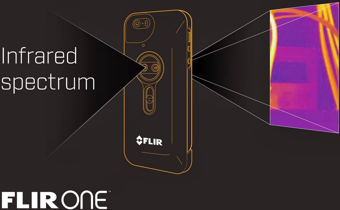
Yamagata TEC will serve as a new production site for CMOS image sensors, and Sony plans to engage in capital investment from the first half of the fiscal year ending March 31, 2015 ("FY14") through the second half of the fiscal year ending March 31, 2016 ("FY15") in order to increase image sensor production capacity. This planned investment is a part of Sony's mid- to long-term plan to increase its total production capacity for image sensors from the current capacity of approximately 60,000 wafers per month to approximately 75,000 wafers per month (in 300mm wafer equivalents). Sony intends to convert part of the semiconductor manufacturing equipment that Sony is scheduled to acquire from Renesas to CMOS image sensor manufacturing, and also to install new equipment for CMOS image sensors. Yamagata TEC will primarily engage in the manufacture of photodiodes and wiring processes for stacked CMOS image sensors.

Sony will position Yamagata TEC as a new site for one phase of the image sensor wafer production process, alongside its existing Kagoshima Technology Center, Kumamoto Technology Center, and Nagasaki Technology Center sites. By doing so, Sony aims to strengthen its capacity to supply stacked CMOS image sensors.

The total investment amount is expected to be approximately 35 billion yen, comprising (i) approximately 7.5 billion yen to acquire Renesas Yamagata Semiconductor's Tsuruoka Factory assets in the fiscal year ending March 31, 2014 ("FY13"), and (ii) approximately 27.5 billion yen for planned capital investment to be carried out during FY14-FY15.

Update: Semicon portal published a nice graphics on the recent Japanese fabs acquisitions. The portal also says that Tsuruoka fab has 40nm process, a nice advance for Sony. There are some challenges for Sony in this deal:

"Renesas moved some of the production equipment to the Naka fab, its main fab, so that it could continue manufacturing game-use system-on-chip LSIs, the Tsuruoka fab's principal products. Sony, therefore, would have to install some production equipment following the contemplated acquisition. This would increase the aggregate investment related to the Tsuruoka fab. Opinion on the advisability of the acquisition is divided within Sony.

From Sony's perspective, another drawback of the Tsuruoka fab is that the production line is not fully automated. Originally designed for high-mix low-volume production, the fab has poor automatic conveyor systems. Therefore, the line could fall short of what is required for highly efficient high-volume manufacturing of CMOS image sensors by Sony.
"

Update #2: Sony publishes a map of its image sensor production facilities:

Tuesday, January 28, 2014

PMD Demos 3D Scanning Application

PMD posted Youtube video showing 3D scanner application based on its recent CamBoard pico XS:

Monday, January 27, 2014

Samsung ISOCELL Technology Webinar

IEEE Tech Insider opens registration for a free Samsung webinar on Feb 11, 2014: "Image Sensors for Mobile Devices: Next Generation Pixel Technology" by Jungchak Ahn, VP of Samsung Electronics’ Image Sensor Product Development, and Marty Agan, Director Engineering in the System LSI business of Samsung Semiconductor.

Samsung presenters will share with the audience how ISOCELL:
  • Decreases crosstalk by approximately 30%, resulting in higher color fidelity
  • Increases the full well capacity by 30%, leading to greater dynamic range
  • Features a 20% wider chief ray, reducing the height of the camera module
They also talk about specific challenges in developing ISOCELL and the solutions that will benefit camera module designs and, ultimately, the end camera applications.

Geo Semi Introduces Single-Chip Wide Angle HDR Camera Processor

GEO Semiconductor introduces the GC6500 family of programmable video processors, integrating GEO’s eWARP core, Apical HDR ISP pipeline, MIPI D-PHY Input, stereo recording path, H.264 Codec, Tensilica XTENSA HIFI CPU and USB2.0 interfaces. Integrated DCDC converters and LDOs provide all necessary system voltages. The eWARP Geometric Processor supports correction for wide field of view lens (180/360). It also supports custom maps for panoramic and zero-content loss views, multiple virtual cameras with perspective correction and ePTZ (electronic Pan, Tilt and Zoom). The processor supports up to 5MP sensor resolution at 30fps and 1080p60 video.

Paul Russo, CEO of GEO Semiconductor says, "There is an explosion of uses for ultra-wide field of view or ‘fisheye’ applications for consumer and industrial markets, such as home security, automotive, cloud and wearable cameras. All of these segments require intense geometric image processing as well as multi-stream compression support. The programmability of the GC6500 provides customers ultimate flexibility and offers H.264 video compression, WDR ISP support in a highly integrated low power IC to enable emerging camera markets. GEO has developed complete software stacks, including iOS and Android applications, to provide superior hardware and software support to its customers and shorten their time to market."

Saturday, January 25, 2014

Eric Fossum Presents CMOS Sensor History in Fermilab

Fermilab publishes Eric Fossum's presentation "CMOS Image Sensors: Tech Transfer from Saturn to your Cell Phone", including an interesting Q&A section in the end, presented on Nov 18, 2013 (via Nuit Blanche blog):


Friday, January 24, 2014

Phase One Features Medium Format Sony Sensor

Cnet, Luminous Landscape, Digital Transitions report that the new Phase One IQ250 medium format digital camera back features 50MP Sony CMOS sensor. The sensor size is 44mm x 33mm (1.3x MF crop factor)and it offers 14-stops DR.

Luminous Landscape also says that the Hasselblad H5D-50C uses the same Sony sensor.

Phase One's Youtube video talks about the new CMOS sensor:

Brigates Announces MCCD Sensors for Security Cameras

Brigates (Chinese name - Rui Kunshan Microelectronics Inc.) announces BG0601 and BG0631 MCCD sensors for PAL-resolution security cameras. MCCD is a CMOS sensor which has CCD-compatible external interface. It be used in place of CCD in security camera, with some modifications: AFE is integrated onto the sensor and HV driver is not needed:

Brigates Chairman Luo Wenzhe presents MCCD technology

e2v on Gaia Sensor

e2v published a PR on its 106 CCDs imager inside the European Space Agency space observatory Gaia on a five year mission to map the galaxy. e2v has implemented different functionalities in each of these CCDs, like charge injection, antiblooming and TDI gate structures to meet the specific needs of the mission. There are three variants of the CCD91-72, each optimised for different wavelengths in the range 250 to 1,000nm. The CCD package is 3 sided buttable, to minimise the dead space between CCDs when they are tiled together in the mosaic and all CCDs have been through e2v’s back thinning process.

Hans Faulks, General Business Unit Manager for Space and Astronomy commented: "We are immensely proud and excited to finally see our image sensors embark on this mission. All the hard work, dedication and expertise that has been put into our sensors and into the mission will finally come to fruition. Our products will now play their part in history as we help increase our understanding of our universe."

Thursday, January 23, 2014

Pelican Imaging News

Pelican Imaging started the new year with quite a few news. First, its website is updated with special emphasis on depth-enabled features:


Second, the company publishes its CTO and co-founder Kartik Venkataraman's keynote on the future of mobile imaging presented at the International Conference on Consumer Electronics (ICCE) on January 12 in Las Vegas, NV. The keynote addresses some of the concerns about the array camera resolution (click to enlarge):


The presentation also talks about the depth-enabled features, after-the-fact focus, background blurring and substitution, videoconferencing, and more. The depth map is not bad for such a small camera:


Third news is that Pelican Imaging's technology has been nominated for a 2014 Edison Award - the nominee #181 out of 309. The winners will be announced on April 30.

New Imaging Technology Unveils Two New WDR Products

New Imaging Technology (NIT) presents its WDR Intensified modules, the first intensified Night Vision cameras with a WDR of more than 140dB. The new WiDy IntenS cameras feature a low power consumption (< 300 mW for the analog version) and a small form factor.


NIT also introduces a new WDR InGaAs products family, including sensors and camera modules. NIT SWIR products are based on a proprietary Wide Dynamic Range ROIC technologies and offer aDR of more than 140dB in a single image.

Wednesday, January 22, 2014

More Market Forecasts from Yole

Yole Developpement's CIS-2014 report sample gives more data from the market report:

Samsung Posts 13MP 1.12um Pixel CIS Flyer

Samsung published a flyer of S5K3L2 13MP, 1.12um BSI pixel sensor which is supposed to end Sony dominance in 13MP sensors for smartphones. The 1/3.06-inch sensor is said to offer the best in class low-light performance:


The sensor is based on 65nm process and consumes "up to 8 percent less power" due to "the smaller and optimized circuit design." The sensor fits to the camera module with z-height of 6mm. Its frame rate is 24fps at full 13MP resolution.

DALSA Explains TDI, Adimec - Blooming and Smear

Educational news: Teledyne DALSA blog publishes a nice TDI mode post with animated explanation. Adimec blog explains blooming and smear effects in CCDs.

Tuesday, January 21, 2014

Kasalis on Expansion Path

Camera module alignment systems maker Kasalis announces that it is expanding and will shortly be tripling its staff and almost tripling its office size. "We are thrilled that our products have struck a chord with manufacturers seeking high quality and cost-effective camera module alignment," said Justin Roe, president of Kasalis. "We grew significantly in 2013, and see this growth accelerating in 2014. Our customers are our top focus, and we will be improving services for them by adding yet more innovative, responsive engineers to our staff and increasing production capabilities. Innovation and speed to market is the key to our success, and we want to further enhance that capability."

Kasalis credits its Pixid camera module alignment systems for its impressive growth. The Pixid’s faster cycle time, lower cost, and faster delivery gives customers the advantage of attaining the lowest cost per part for actively aligned small camera modules and array cameras, and the ability to quickly bring new products to market.

New HTC One to Feature Twin Rear Camera

Bloomberg reports that the upcoming new version of HTC One smartphone will have "twin-sensor rear camera" featuring "better focus, depth of field and image quality". Bloombers source call it "an improved version of HTC’s Ultrapixel camera". Phonearena speculates that this could be the recently announced Toshiba stereo camera module.

Thanks to DM for the link!

Hasselblad to Switch to CMOS Sensors

Hasselblad is to launch what it calls "the world's first 50MP medium format camera using CMOS sensor technology" in March 2014.
Ove Bengtson, Hasselblad Product Manager said: "This pioneering 50 megapixel CMOS sensor camera is based on our H5D-50 model but will offer a faster capture rate; longer shutter speed capability and much greater ISO performance. It will provide greatly improved Live Video in Phocus and will also be available with Multi-Shot functionality."

Hasselblad's new CEO Ian Rawcliffe said: "This is a world-first and underpins Hasselblad's status at the forefront of camera technology. It will be the first of a number of medium format capture innovations we have planned for the coming months."

Monday, January 20, 2014

Yole Updates CIS Market Report

Yole Developpement announces an updated image sensor market report and forecast. Few of the announced key points:
  • Driven by handset and tablet applications, a 10% CAGR is forecast for the CMOS image sensor market from 2013 – 2018, reaching a value of almost US$13B by 2018.
  • Big 3, Omnivision, Samsung and Sony, will continue to dominate thanks to advanced technologies, a large installed capacity and a cost-optimized manufacturing machine, while second-tier players must overcome economic and technical challenges to stay competitive.
  • The strong move in the CIS markets from major player such as Sony’s pushes other companies to a fablight / fabless strategy. Indeed, this evolution has started already with companies like Aptina and STMicroelectronics. Besides a dramatic change in their business model, these players also move to higher end applications and out of the traditional mobile phone market.
  • Three years after its introduction by Sony and Omnivision, BSI image sensors accounted for 27% of total CIS sales in 2012. BSI’s adoption is expected to reach more than 78% in 2018, bringing its total revenue to $10B.
  • The current batch of breakthrough CMOS image sensor technologies aim to:
    - Diminish thickness (module level)
    - Improve image sensor performance (i.e. QE, sensitivity, resolution, reduced cross-talk, higher DR, multispectral imaging, faster processing, larger CRA, lower power consumption)
    - Permit new functions (i.e. post/fast focus, photon discrimination, 3D imaging, gesture recognition, increased processing power).
CIS Market Forecast

Sunday, January 19, 2014

Camera Module Image Quality Testing

Photonics Spectra publishes an article on camera module image quality testing. The article is quite concise and mainly talks about the advantages of collimator domes over the illuminated test chart setups:

Illuminated Test Chart Setup
Collimator Setup

The collimator setup advantages are:
  • can be used as a “true” infinite setup, with the DUT being tested under the same conditions as in the final application. This setup is quite insensitive to the actual positioning of the collimators, as the field positions are determined only by the angles between the collimators.
  • The test chamber is compact, with the outer dimensions independent of the DUT field of view, so it uses less factory floor and is easier to manage.
  • less sensitive to stray light, and the reticle illumination can be better controlled, leads to better repeatability.
  • By using motorized collimators that can be focused, arbitrary object distances from approximately 1 m to infinity can be generated. This makes it possible to test the focusing of fixed- and autofocus modules. It is further important for the high-precision active alignment technology.

Saturday, January 18, 2014

JRC Identifies Sensors by Noise

European Commission Joint Research Centre (JRC): Recent advances on image processing allow identification of which device has taken a given picture, and allow a match with those contained in social network accounts (Facebook, Flickr, etc.). This possibility has been demonstrated in a recent JRC study that received the Best Paper Award at the International Conference on Computer Vision Theory and Applications (VISAPP 2014) in Lisbon, Portugal this January:

"On the usage of Sensor Pattern Noise for Picture-to-Identity linking through social network accounts"
Riccardo Satta and Pasquale Stirparo

JRC exploited the noise pattern that is left in a digital picture by any image sensor, as a fingerprint of the imaging device (whether it is a digital camera, a smartphone, a tablet, …). Such a Sensor Pattern Noise (SPN) has been shown to be unique for every single device. This allows one to find, given a picture, a social network account containing images taken by the same camera, and in turn it can be possible to infer the identity of the camera owner.

Friday, January 17, 2014

PMD Presents World's Smallest ToF Camera

PMD presented its new CamBoard pico XS in private suite at CES, together with PMD's middleware nimble UX. The company says that it's the smallest depth sensor worldwide, as far as they know. Its key specs:

  • The size of the pico XS is 4mm x 15.5mm x 39.5mm.
  • It uses a laser illumination, 850nm and modulation frequency of 80MHz.
  • It´s equipped with a standard MIPI compliant interface - ready for integration into devices.
  • Self heating is only up to 10° C
  • Power consumption is typically < 50mW (max 350mW)

Engadget publishes a video from the private demo:


Fujifilm Proposes RGBW Pixels with Different Size

Japan-language Egami blog reports that Fujifilm applies for a Japanese patent 2013-258168 on different-sized RGBW filter pattern. The green and white pixels are bigger to minimize the luminance noise at the expense of chrominance noise elevation. YourNewsTicker nicely painted the B&W figure from the application:

Fairchild Imaging to Unveil sCMOS 2.0 Sensors

BAE Fairchild Imaging sends email invitations to its Photonics West booth on Feb 2-6, 2014, saying:

"We will be launching our next generation of sCMOS high performance CMOS image sensors: sCMOS 2.0. With the launch of sCMOS 2.0, we will bring the best of image sensor technologies that are ideally suited for the scientific camera market."

Thanks to BP for the info!

Thursday, January 16, 2014

Analysts Skeptical on Array Camera Market

Maybank Kim Eng (Korea) and Core Pacific Yamaichi (Hong Kong) published reports on Sunny Optical developing its own array camera, similar to Pelican's.

Core Pacific says: "we do have a number of concerns.

(1) High setup cost. To build a production line on active alignment components, some special machines and equipment are required, resulting in hefty CAPEX caused by depreciation. Besides, the technology is new meaning that more investment on R&D has to be made and the immature supply chain also leads to high sourcing costs for related components.

(2) Concern on technology knowhow. Sunny tends to develop its own production line on active alignment based on its R&D capacity. Although its technology knowhow is leading in the domestic market, it is still lagging behind those international players in Taiwan, Japan and Korea. We doubt whether its quality can be up to the international standard.

(3) Difficult to achieve the accreditation from first-tier global smartphone brands. We believe it still takes years for array camera to be mature. Before that the production cost is expect to remain high, implying that only high-end smartphone models, such as iPhone and Galaxy S Series, can absorb this cost. However, the entry barrier of these flagship models’ supply chain is extremely high. Sunny has no global footprints on HCM and the quality control is relatively weak comparing to the international peers. Whether or how long Sunny can achieve the accreditation of first-tier global smartphone brands remains in doubt.

So far, the visibility on array cameras business is low and we do not expect it to make contribution till FY15F.
"

Maybank writes: "Although array camera can provide a thinner design, quicker photo-taking response time and can refocus on multiple subjects on the phone, we think the adoption rate of array cameras will remain low in 2014 owing to its inferior photo quality in the near range and long range, and higher cost due to low production yield rates. So far, only several projects among the Chinese brand names and Nokia show an interest in adopting the array camera (meaning demand is not strong). In addition, our checks indicate that LiteOn can also offer a very competitive array camera design if its customers want to use it (suggesting another good array camera supplier)".

Another interesting quote from Maybank report is that, according to consumer survey by O2 in 2012, picture taking is the most used function in mobile phones:

Tessera to Cease All Remaining mems|cam Manufacturing Operations

Business Wire: Tessera is restructuring its DigitalOptics business (DOC) to cease its remaining manufacturing operations and refocus on monetizing DOC technologies, including solutions for imaging and MEMS technologies. These actions are the culmination of an in-depth review of strategic alternatives for DOC that was conducted in conjunction with the Company’s financial advisors, the newly reconstituted board of directors and the new senior management team. As a result of the restructuring, the Company expects its quarterly DOC related operating expenses to be reduced by approximately $17 million, realized in full by the third quarter of 2014.

Tom Lacey, Tessera’s CEO, commented, "After an exhaustive process of exploring multiple options, we have decided to cease DOC manufacturing operations and focus our resources in DOC on continuing to operate our image enhancement business, while also exploring new ways to realize value from our extensive DOC intellectual property portfolio, including a sale, licensing or other means. While the strategic process ultimately did not lead to a sale of the mems|cam business, we achieved solid proof of concept by demonstrating working mems|cam camera modules, including shipping pre-production units that generated substantial customer interest. We strongly believe that there is significant value in the related intellectual property that has been developed, including our camera module, MEMS, and image enhancement technologies. Additionally, we continue to believe our mems|cam technology is unique and novel and may be incorporated into mobile devices in the future. To that end, we intend to maintain a small team of MEMS engineers to further the mems|cam technology and pursue possible avenues to unlock the value of this powerful technology."

Thanks to SF and SC for sending me the news!

Wednesday, January 15, 2014

SK Hynix Update

SK Hynix has updated its image sensor product page showing its current offerings and plans:

Tuesday, January 14, 2014

Qualcomm Demos Multiple Capture and Fusion

Techcrunch video shows Qualcomm SnapDragon 805 photography capabilities, one of them being Lytro-like re-focus feature:


Dongbu Supplies Sensors to Brigates

Business Wire: Dongbu has begun supplying CCTV image sensors to Brigates, a fabless Chinese company. Currently supplying Brigates with D1 resolution sensors (0.44MP), Dongbu expects to develop higher HD 720P resolution sensors with Brigates in the second half of this year.

China’s interest in CCTV surveillance may be increasing due in part to the mainland hosting more and more international events such as Shanghai Expo and the Guangzhou Asian Games. According to some estimates, the Chinese CCTV market has steadily grown from 47.5 billion yuan in 2009 to 65 billion yuan (about US$10.7 billion) in 2012.

JungChak Ahn Promoted to VP at Samsung

JungChak Ahn, image sensor technology leader at Samsung, and a member of Image Sensor Workshop and ISSCC technical committees has been promoted to VP position at Samsung, as his LinkedIn page updates. JungChak will present at Image Sensors conference in London in March 2013.

Sunday, January 12, 2014

Interview with Pelican Imaging CEO

GeekBeatTV published a Youtube video interview with Chris Pickett, CEO of Pelican Imaging:

Friday, January 10, 2014

7th Fraunhofer IMS Workshop on CMOS Imaging: From Photon to Camera

The 7th Fraunhofer IMS Workshop on CMOS Imaging takes place in Duisburg, Germany, on May 20-21, 2014. The content of the workshop is thematically dedicated to extended spectrum imagers, SPADs, detector technologies, as well as cameras and applications. Fraunhofer IMS is expecting about 100 participants from all over the world who are active in all fields of CMOS imaging. Visit of Fraunhofer IMS wafer fab is possible. The list of presentations is below:
  • Fundamentals of CMOS Imaging: the Pinned Photodiode
    Albert Theuwissen, Harvest Imaging
  • Evolution and Limitations for Mobile Image Sensors
    Robert Gove, Aptina
  • CMOS Imagers for Digital Still Cameras
    Guy Meynants, CMOSIS
  • SWIR InGaAs FPAs for Passive and Active Day & Night Vision
    Jan Vermeiren, Xenics
  • Hyperspectral Imagers
    Piet de Moor, IMEC
  • SPADs for Single-Photon Imaging in the Near Infrared
    Alberto Tosi, Politecnico di Milano
  • CMOS Technology for SPAD/SiPM
    Daniel Durini, FZ Jülich
  • SPAD-Based ToF-Imaging for Automotive Safety Applications
    Christiano Niclass, Toyota Central R&D Labs
  • CMOS Spectroscopy Using LDPDs
    Werner Brockherde, Fraunhofer IMS
  • Silicon X-Ray Detectors - in Heaven and on Earth
    Lothar Strüder, PNSensor
  • Merging Technologies for Multi-Aperture Cameras
    Andreas Bräuer, Fraunhofer IOF
  • Lightfield Cameras
    Christian Perwaß, Raytrix
  • Computational Imaging for Industrial Applications
    Svorad Å tolc, AIT Austrian Institute of Technology
  • Industrial Cameras
    Jochem Herrmann, Adimec
  • High Resolution Earth Observation Cameras
    Andreas Eckart, DLR

DisplaySearch Forecasts 330M Gesture-Controlled Devices in 2015

NPD DisplaySearch analysts believe that nearly 330M smart devices with gesture-sensing will be shipped in 2015, about 70% increase over the 2014 forecast and a doubling of shipments in 2013. The adoption of 3D depth sensing becomes more accurate and affordable, not only on smartphones and tablets, but also on smart TVs, all-in-one PCs, and other large-screen devices.

Shipment Forecast for Gesture Sensing Solutions
for Smart Devices. Source: NPD DisplaySearch

"Gesture sensing is the next critical user interface trend, designed to improve the usefulness of, and user experience on, smart TVs and other large smart devices," says Calvin Hsieh, research director at NPD DisplaySearch.

The recent and planned use of 3D gesture-sensing technologies in connected smart devices includes the following:
  • Mobile devices have touch screens and microelectromechanical systems (MEMS) as major user interfaces, but gesture sensing exists as a supportive user interface.
  • Smart TVs and other larger devices cannot leverage touch screens, which is why Samsung and other TV makers are now beginning to offer gesture sensing technologies in upcoming products.
  • Game consoles (e.g., Xbox and PlayStation 4) already rely primarily on 3D gesture-sensing controls.
  • PCs have not leveraged gesture sensing widely. However, Intel has proposed perceptual computing as the next dynamic for PCs in 2012.
Over the past year alone, Intel acquired Omek (gesture middleware vendor); Microsoft released the new Kinect with TOF technology for Xbox One; Sony adopted stereo vision for the new PS Camera for PlayStation 4; Apple acquired PrimeSense for its structured light technology, which could be used on future Apple TVs; and Google acquired Flutter. Also, Samsung has been applying gesture sensing to their smart TVs for the past two years.

Thursday, January 09, 2014

Point Grey Promotes Sony Global Shutter Technology

Point Grey's December 2013 newsletter promotes its new 1920x1200 camera with Sony IMX174 global shutter sensor, for the first time featuring in Grasshopper3 GS3-U3-23S6M-C camera:


"To achieve optimal imaging performance, Sony’s special “analog memory” perfectly stores and shields the light collected in the photodiode. This technology minimizes common global shutter CMOS artifacts such as fixed pattern noise and dramatically lowers read noise levels to just 7 electrons (e-). The IMX174 sensor further boasts saturation (full well) capacity of 32,000 electrons (e-), dynamic range of 73 dB, and peak quantum efficiency of 76% at 525 nm."

Wednesday, January 08, 2014

Intel Presents its Own 3D Camera

VentureBeat: Intel presents its own 3D depth sensing camera at CES, called RealSense 3D, a part of Perceptual Computing program. Little is said about the camera technology. Intel just says that it features "full 1080p color and a best-in-class depth sensor, the camera gives PCs and tablets 3D vision for new, immersive experiences. Interact more intuitively with facial recognition, emotion tracking, 3D scanning, and background extraction, or use 10-finger gesture recognition for agile device control." VentureBeat publishes a blurry picture of the camera board:

2gig Image Sensor for $108.97

A funny item is being sold on Amazon: "2gig Image Sensor Digital Still Camera" for $108.97. 2gig is a name of the company. The actual resolution is QVGA.

Softkinetic News

PR Newswire: SoftKinetic's DepthSense 3D ToF USB camera and iisu gesture recognition middleware have been integrated with the NVIDIA Tegra NOTE 7 tablet platform, and the platform is available to developers to create 3D depth sensor-enabled applications for the mobile world. The Tegra NOTE 7 is powered by the Tegra 4 mobile processor, which features a 72 custom core GPU and quad-core ARM Cortex-A15, plus a second-generation battery-saver core. SoftKinetic's middleware and camera hardware will enable Tegra NOTE 7 to provide short range 3D gesture tracking and real-time 3D depth sensing, as close as 6 inches away at up to 60 fps.

PR Newswire: SoftKinetic unveiles an in-vehicle, gesture-based infotainment solution based on SoftKinetic technologies and Freescale silicon. "Freescale is committed to providing the most innovative embedded processing solutions for the automotive industry, and gesture recognition is a vital part of that strategy," said Rajeev Kumar, director of marketing and business development with Freescale's MCU business. "SoftKinetic's solutions for 3D vision offer the extremely sophisticated capabilities which help our shared customers innovative 3D embedded automotive solutions."

PR Newswire: MakerBot, the leader in desktop 3D printing, and SoftKinetic jointly announce a strategic partnership. This partnership is expected to help MakerBot expand its 3D Ecosystem and 3D Printing Platform, and enhance the ease of use and connectivity of MakerBot Replicator Desktop 3D Printers and Scanners. SoftKinetic will enhance its 3D camera technology for 3D scanning. SoftKinetic is focused on the development of next generation 3D cameras based on its technology for inclusion in future MakerBot 3D scanning products.

Tuesday, January 07, 2014

Omnivision Announces Distortion Correction Chip For Automotive Camera

PR Newswire: OmniVision announces immediate availability of OV480, a distortion correction chip for wide FOV automotive applications. It is currently shipping to multiple global tier-1 automotive suppliers. The OV480 can correct lens distortion of up to 195-degrees and enable rear-view and 360-degree surround view systems. Additionally, the OV480 supports a cross-traffic view, which allows drivers to view traffic from both sides of the vehicle.

DxO Licenses its ISP to Anapass

DXO Labs announces that it has licensed its ISP to Korea-based Anapass Inc.

"We are very pleased to team up with DxO Labs, the reference company for image quality, to bring up Anapass application processors," says Kyeong Ho Lee, CEO, Anapass Inc. "The DxO ISP will offer to our mobile application customers its high-performing image pipeline along with his great expertise, delivering cameras with stunning images and great quality videos."

"We are excited to partner with Anapass to bring to market our latest generation of DxO ISP camera image processing hardware" says Jerôme Ménière, Chairman and CEO of DxO Labs. "The camera system is an essential feature of a mobile device. End-users are now considering their smartphones as their primary camera. Only DxO, with its years-long experience in designing imaging pipelines for DSLR, digital compact and smartphone cameras, can deliver a complete high-end solution for mobile device’s camera sub-system."

FLIR Announces First Consumer Thermal Camera

FLIR announces FLIR One - a $350 thermal imaging camera that clips on back of iPhone 5 or 5s:


The camera has two sensors - an IR one with unknown resolution and a visible light VGA sensor that "adds visible spectrum detail to thermal images and enhances resolution":


A promotional Youtube video talks about the new camera applications:


Thanks to SF for the link!

Update: FLIR also announces Lepton thermal imaging camera core - similar in size, weight, and power consumption to a conventional CMOS cell phone camera module, said to be the world's smallest microbolometer-based thermal imaging camera core currently available. Lepton is used in FLIR One camera. It has "a breakthrough lens fabricated in wafer form, a microbolometer FPA, and advanced thermal image processing on an ASIC. Lepton is fully compatible with FLIR’s patented multi-spectral imaging (MSX) technology, which allows visible and thermal image streams to be combined for sharper, more visually pleasing hybrid images."

FLIR Lepton Module