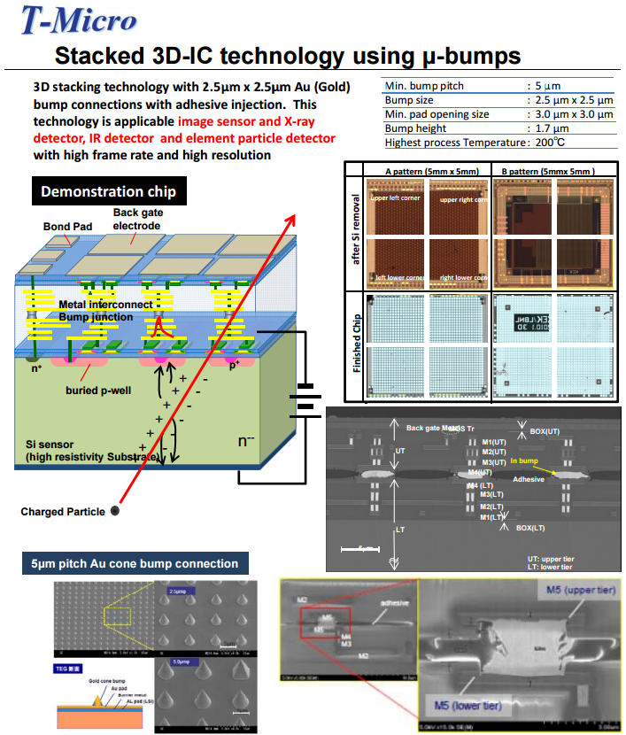
Friday, July 31, 2015

Hutchinson Introduces SMA OIS Actuator

GlobeNewsWire: Hutchinson expects to begin shipping prototypes of a new Cambridge Mechatronics' Shape Memory Alloy Optical Image Stabilization (SMA OIS) actuator to tier 1 camera module manufacturers in early August. The new Gemini product was designed in response to customer requests for reduced OIS camera thickness. Gemini is said to reduce SMA OIS actuator thickness by more than 70%, to enable the world's slimmest OIS smartphone cameras. Gemini is expected to be ready for volume production in Q4 2015.


Building on the value users place on "selfie" photos, Hutchinson Technology is also developing SMA OIS designs to improve front-facing camera image quality. Front-facing SMA OIS samples are also expected to be available in Q4 2015.

Meanwhile, the UK-based Cambridge Mechatronics that has licensed its technology to Hutchinson reports that its smart metal OIS camera was launched in InFocus M530 smartphone in India.

Omnivision Presents New VGA Sensors

PRNewswire: OmniVision announces the cost-optimized and power-efficient OVM7699 CameraCubeChip and OV7699 CameraChip based on 1.75um OmniBSI+ pixel. The 1/13-inch OVM7699 and OV7699 are said to have the industry's smallest footprint and intended for a wide range of applications, including feature phones, mainstream smartphones, notebooks, wearables and IoT devices, among others.

The OVM7699 comes in a 2.1 mm x 2.1 mm CameraCubeChip™ module with a z-height of approximately 2.3 mm, while the OV7699 comes in a 2.03 mm x 2.08 mm CSP. Both the OVM7699 and the OV7699 are currently available for sampling, and are expected to enter volume production in Q1 2016.

ON Semi Announces Automotive ISPs

BusinessWire: ON Semiconductor introduces a new series of image co-processors for 1080p HDR automotive cameras. Designed to work in conjunction with the company’s 2MP and 1.2MP image sensor devices, the new AP020x series of co-processors enable a range of solutions for automotive rear view and surround view cameras. The new image co-processors all incorporate an HDR color pipeline with adaptive local tone mapping (ALTM).

  • The AP0200AT image co-processor is optimized for rear view cameras and offers Ethernet output. It also includes a spatial transform engine (STE), which enables lens distortion correction and de-warping, as well as a sophisticated overlay graphics engine.
  • The AP0201AT also has Ethernet output and is aimed at Ethernet-based surround view.
  • The AP0202AT is targeted at digital surround view and utilizes a 24-bit parallel output.
  • The AP0102AT is targeted at 1 MP/720p rear view cams, and includes the STE and overlay graphics engine

Thursday, July 30, 2015

Light Closes $25M Series B Financing

Light has raised a $25M Series B round of funding. All of Light existing investors participated in this round, in addition to new investors Formation 8, which led the round, and StepStone. This brings Light’s total funding to around $35M.

The Light camera prototypes are now up and running. The company has doubled the size of its team in the last three months and plans to double it again before the end of the year.

Forbes publishes an article on the Light's financing round:

"The way Light’s camera technology works is by placing multiple cameras on the back of a phone — around 6 or 11 cameras. Light stitches together all those images with its software to come out with high-resolution photos. Depending on how many cameras the phone maker chooses, it can achieve between 32 megapixels and 52 megapixels.

Light’s cameras can also zoom using what’s called folded optics, which is a method of bending light to make the camera’s size requirements more compact. Light can zoom between 70 millimeter and 150mm.

The Light module is paired with a Snapdragon application processor from Qualcomm.
"

"The build of material costs will be at least $60 for phone makers to add Light’s technology, but [Light CEO] Grannan points out that that’s nothing compared to having to shell out $2,000 for a nice DSLR camera."

"Light expects the first phones to come out with its camera will be in 2016."

Light camera-phone

Toshiba Unveils PDAF-Equipped Sensor Lineup

BusinessWire, PRNewswire: After presenting its first image sensor with PDAF 2 weeks ago, Toshiba announces a full lineup of these sensors, all based on 1.12um BSI pixels. The part numbers of the new sensors are same as the previously announced ones, but with -121 suffix to indicate a PDAF-enabled version:


Sample shipments of devices in the series will start in August, and they will be rolled out in turn.

Sony Reports Another Increase in Image Sensor Sales

Sony reports its quarterly results for the quarter ended on June 30, 2015. Few quotes:

"[Sony Devices Segment] Sales increased 35.1% year-on-year (an 18% increase on a constant currency basis) to 237.9 billion yen (1,950 million U.S. dollars). This increase was primarily due to a significant increase in sales of image sensors reflecting higher demand for image sensors for mobile products, the impact of foreign exchange rates, as well as a significant increase in sales of camera modules. Sales to external customers increased 41.2% year-on-year.

Operating income increased 18.8 billion yen year-on-year to 30.3 billion yen (249 million U.S. dollars). This significant increase was primarily due to the impact of the above-mentioned increase in sales of image sensors and the positive impact of foreign exchange rates.
"


Update: Sony publishes an updated Semiconductor Business Flyer:

Canon Commercializes its ISO 4,000,000 FF Image Sensor

BusinessWire: Canon introduces its first multi-purpose camera, the new ME20F-SH, with exceptionally high sensitivity to capture Full HD video with a minimum subject illumination of less than 0.0005 lux (color, no light accumulation, f/1.2, 30P fps, 50 IRE, at maximum 75 dB gain setting, equivalent to an ISO sensitivity of over 4,000,000). Nighttime surveillance and security, cinematic production, reality television, and nature/wildlife documentaries are just some of the ME20F-SH’s many possible usage applications.

Canon’s new multi-purpose camera employs an enhanced version of the 35mm full-frame CMOS sensor that was originally developed in 2013. The ME20F-SH sensor has pixels measuring 19 μm, said to be more than 5.5 times the surface area of the pixels on the CMOS sensor featured in select top-of-the-line interchangeable lens cameras. Furthermore, the sensor’s pixels and readout circuitry make use of Canon proprietary technologies to achieve both reduced noise and exceptionally high sensitivity on subjects with a minimum illumination of less than 0.0005 lux. This multi-purpose camera allows users to discern subjects under even some of the dimmest lighting conditions, such as environments lit by artificial illumination or under a moonless night sky. Furthermore, similar to Canon’s Cinema EOS System of professional digital cinematography cameras, the ME20F-SH camera includes Canon Log and Wide DR.

ME20F-SH is expected to be available in December 2015 at a suggested retail price of $30,000.


A DSLR comparison picture from Canon Japan site:


Canon plans to make sample images avaliable in Sept 2015 on this link.

Wednesday, July 29, 2015

Nokia OZO Combines Eight Cameras into One

Nokia announces OZO, said to be the first commercially available VR camera designed and built for professional content creators and the first in a planned portfolio of digital media solutions from Nokia Technologies, the company's advanced technology and licensing business. Conceived at the company's R&D facilities in Tampere, Finland, OZO captures stereoscopic 3D video through eight synchronized global shutter sensors and spatial audio through eight integrated microphones.


Verge shows many pictures from the new camera presentation in LA:

Samsung Enters Mass Production of 1um Pixels

BusinessWire: Samsung announces the industry’s first 1.0μm-pixel-based 16MP sensor for mobile devices. The new S5K3P3 leverages the company’s ISOCELL pixel technology.

As a trendsetter in the mobile image sensor business, we are pleased to be the first to deliver the most advanced 1.0μm-pixel imager, which meets both high-resolution and slim design requirements for smartphone cameras,” said Kyushik Hong, VP and Head of S.LSI Marketing at Samsung Electronics. “Starting with 16Mp sensor, Samsung plans to further expand 1.0μm-pixel product category and lead the image sensor market for high performing slim mobile devices.

Built with 1.0μm pixels, the new 16MP image sensor reduces the module’s overall height by 20%, compared to current 1.12μm-pixel based 16MP sensor modules, enabling a module z-height that is less than 5mm.

In addition, the S5K3P3 takes advantage of Samsung’s ISOCELL technology to deliver image quality that is on par with 1.12μm-pixel based image sensors. Using ISOCELL technology reduces color crosstalk of neighboring pixels by adding physical barriers between each pixel.


Meanwhile, the newly announced OnePlus 2 smartphone goes in the opposite direction and uses larger 1.3um pixels in its 13MP sensor from Omnivision. The phone also has laser-assisted 200ms-fast AF:

"Despite being a go-to measure for smartphone cameras, megapixels fail to tell the whole story. The true test of a camera is the quality of its image sensor and optics. Our sensor contains large 1.3µm light-collecting pixels—the biggest ever in a 13MP smartphone camera—for unmatched low-light performance."

Tuesday, July 28, 2015

Intel RealSense Front Camera Reverse Engineering

Chipworks publishes a report on Intel structured light RealSense camera reverse engineering.


The front-looking camera uses changing light pattern projected through ST-manufactured MEMS mirror:


The RealSense's IR image sensor has a lot of circuits around the pixel array:

Intro to 2nd Generation Sony Global Shutter Sensors

Point Grey publishes a nice Youtube video explaining the differences between 1st and 2nd generations of Sony Pregius CMOS sensors:

Monday, July 27, 2015

Rumor: Qualcomm Vuforia Group is Up for Sale

One of the recent rumors I got: "As a part of QCOM's restructuring efforts announced this week, the Vuforia team is being put up for sale. After the Metaio-Apple purchase, which took a key client opportunity off the table, and with Google Android with their own internal solution, it is not surprising that QCOM management would make this move as a part of their restructuring efforts."

Just over a month ago, Vuforia won Auggie Award: "The Qualcomm Vuforia mobile vision platform won an Auggie Award for “Best Tool” for the third year in a row at this year’s sixth annual Augmented World Expo (AWE). Hosted by AugmentedReality.org, AWE celebrates wearable computing, gesture devices, the Internet of Everything, and of course, augmented reality (AR)."

The company's Vuforia Youtube channel has a lot of demos of the platform:

Saturday, July 25, 2015

Pelican Imaging Layoffs?

Somebody posted in comments that Pelican Imaging has just layed off most of the company. Whether this is true or not, their technology page points to a big shift in direction: instead of being a main camera for smartphone, the company now proposes a supplementary camera array for just a depth map:

"This unique "array + main camera" approach allows mobile handset manufacturers to choose their own primary camera module (whether it’s 8MP, 13MP, or 20MP), and benefit from excellent image quality paired with the depth data from the scene."


Update: EETimes confirms the layoffs:

"The company said that approximately half the staffing of 25 was let go.

A spokesperson for Pelican Imaging confirmed that the company has "reduced some of its staff recently, to allow the company to focus on core product development."

"Regrettably, Mark Fulks has left the team at Pelican. Mark is a very well respected leader and we wish him success in his next endeavour," the spokesperson said.
"

Friday, July 24, 2015

Omnivision's Stockholders Approve Acquisition

PRNewswire: OmniVision's stockholders approved the Agreement and Plan of Merger of OmniVision, Seagull International Limited and Seagull Acquisition Corporation. Seagull International Limited and Seagull Acquisition Corporation are affiliates of a consortium composed of Hua Capital Management Co., Ltd., CITIC Capital Holdings Limited and GoldStone Investment Co., Ltd.

Under the terms of the Merger Agreement, stockholders of OmniVision will receive a total of approximately $1.9 billion. The transaction, which is expected to close in the third or fourth fiscal quarter of fiscal year 2016, is subject to regulatory approvals, including antitrust review in the U.S. and the People's Republic of China, review and clearance by the Committee on Foreign Investment in the U.S., clearance or approval under applicable Taiwan law, and other customary closing conditions. In order to obtain clearance or approval under applicable Taiwan law, OmniVision will divest certain of its investments in Taiwan, including certain of its interests in a joint venture.

Sony Proposes 2-layer Stacked PDAF

SonyAlphaRumors quotes Japanese-language Egami blog describing a new Sony patent application - a 2-layer image sensor having RGB pixels on top, and PDAF pixels on the bottom. I guess PDAF layer only gets IR and residuals of red image from the top RGB layer:


Thanks to TG for the link!

Thursday, July 23, 2015

ST Imaging Business Update

SeekingAlpha: ST Q2 2015 earnings call transcript has few details on ST imaging business:

Carlo Bozotti - President, CEO:

"I think now, Carlo, do we have this exact some of the camera modules. I think this is a business that we have decided to phase-out. So, we are moving from $20 million to $25 million per quarter in - $20 million per quarter for in Q4 last year. Well, this is the order of, we try to give you the precise number but this is a business that for last year was about $20 million and is going to be zero because of the phase-out that we have decided by Q4 this year. So, very close to zero, so, this is the impact of the phase-out of this part.

I have to say that in this unit, we also have the forma ST had some products that are also being phased out. So, now for us to after the discussion we had one quarter ago certain new opportunities that did not materialize. Of course for us remaining flat means to replace this business that is phasing out with new products.
"

"In other area, that is contributing to this growth is what we call Baby-Bear or the Time-of-Flight silicon photonics, this is now becoming more pervasive in Asia, particularly in the area so far but we have new opportunities of auto-focusing. So and is we have now a number of phone-makers in Asia that are using this new technology for a better out-of-focus.

I have, I think I have got the number here for the overall camera module business, I suppose this was in Q4 last year, right?
"

Carlo Ferro - CFO:

"No, this is $20 million Carlo, is the reduction in revenues from Q2 ‘14 to Q2 ‘15."

"And then, this is $28 million while the overall image business that decline revenues by $9 million in the same period."

Carlo Bozotti - President, CEO:

"So, in one year on this, in the last 12 months let’s say this camera module business, we lost about $30 million. And I think we have another $10 million or so to go but it will be zero in Q4 this year."

Guenther Hollfelder - Baader:

"The image sensors for automobiles."

Carlo Bozotti - President, CEO:

"Well, I think this is the kind of diversification that we want to push you. I think yesterday I was at major carmakers and say that our sensors is introduction and this is differentiated, of course it’s not a commodity camera module, it’s a differentiated imaging device and that is integral part of our system around advanced safety. And as you know, you need sensors on the car to monitor.

So it’s certainly is an important area. We also have image signal processing solutions for automotive applications. So it is a massive effort, this one around advanced safety. It’s close to our corporation with Mobileye but it’s also this special image-sensor for automotive is our ISP for automotive applications is very much centered on our FD SOI technology. And I think is certainly one area of priority for ST. But to be specific on the camera, we had introduction already.
"

Caeleste Gets New Business Development Manager

Jan Vermeiren joins Caeleste as a Business development manager. Jan has a long career in image sensor design and technology as well as in business development. He has more than 25 years of experience with CCD and CMOS image sensors (design, test & characterization, implementation), process development (CCD, CMOS and backend processes for imagers and FPA’s), Infrared FPA developments, including cryogenic circuit operation, radiation effects on detectors and circuits, camera development and a broad interest in imaging applications and spectroscopy. He also operated in an international context for bi-lateral or multi-party projects and programs.

"Eye on Sensors" Blog

Andrew Burt, Toshiba America's VP of Image Sensor Business Unit, starts "Eye on Sensors" blog. The first post is devoted to the automotive image sensor market:

Wednesday, July 22, 2015

Sony Posts RGBW Sensor Flyer

Sony publishes 1/3.06-inch 13MP, 1.12um pixel IMX278 sensor flyer. Chipworks has found it inside Huawei P8 smartphone. Other than internal RGBW to Bayer re-mosaic block, the new sensor features "Dual sensor synchronization operation." Possibly, Sony prepares to the wide use of dual sensors in smartphones.

Functions and Features:
  • Stacked CMOS image sensor Exmor RS
  • 1.12um pixel
  • RGBW coding color filter and RGB primary color mosaic reproduction on chip
  • Super High SNR and Advanced Noise Reduction for white remosaic
  • Full resolution @30 frame/s (Normal). 4K2K @30 frame/s (Normal)
  • Lens Shading Correction
  • 2-wire serial communication (I2C “Fast mode Plus” is also supported)
  • Output video format of RAW10/8, COMP8
  • Independent flipping and mirroring
  • CSI-2 serial data output (MIPI 2lane/4lane, Max. 1.2 Gbps/lane )
  • Dual sensor synchronization operation
  • Power-on reset function
  • 7.168 K bit of OTP ROM for users
  • Built-in temperature sensor

Movidius' Myriad 2 Wins EETimes ACE Award

EETimes and EDN announce their joint 2015 Annual Creativity in Electronics (ACE) Awards. About the only imaging device in the long list of awardees is Movidius Myriad 2 vision processor. The 28nm processor features 12 MIPI lanes to connect to up to six 1080p60 cameras, and is said to consume less than 500mW.

It can be used in a number of applications:
  • Computational photography (rapid autofocus, HDR, extreme low light)
  • 3D modeling & scanning
  • Indoor navigation
  • 360-degree panoramic video
  • Visual analytics
  • Immersive gaming, augmented reality
  • Gesture recognition
  • Always-on face and object detection
  • Industrial vision

Tuesday, July 21, 2015

Awaiba Germany Changes its Office and Name

CMOSIS reports AWAIBA GmbH has moved to the new larger facilities providing 800 m² office and lab area including a new an 80 m² cleanroom. Also, the name of AWAIBA GmbH has been changed to CMOSIS Germany GmbH in order to stress the ongoing integration of the business in the CMOSIS group.

T-Micro Offers Au-bump 3D Stacking Process

Tohoku University, Japan, spin-off Tohoku-Microtec Co. (T-Micro) offers gold bump stacking process for 3D image sensor integration:

Monday, July 20, 2015

Panasonic Presents 3D Photolab with 120 Cameras

Panasonic presents 3D Photolab with 120 Lumix GH4 cameras to instantly create a 3D model of the subject. A Youtube video shows how this can be a future of studio photography:

Saturday, July 18, 2015

Court Rejects Class Actions Against Omnivision Buyout

PRNewswire: A number of class action lawsuits related to the Seagull Acquisition Corporation's merger with OmniVision have been filed in the Superior Court of the State of California. On July 16, 2105, the Court held a hearing on that motion. Following the hearing, the Court denied, in its entirety, plaintiffs' motion seeking to enjoin the Merger.

10Mfps QVGA Camera Uses Tohoku University's Image Sensor

Tohoku University, Japan reports that Prof. Shigetoshi Sugawa's research group in cooperation with Shimadzu Corporation has developed an 10 million frames per second image sensor with ISO 16,000 sensitivity. An ultra-high-speed video camera incorporating the developed CMOS image sensor is newly released by Shimadzu Corp. The new sensor which offers six times higher photosensitivity over the previous generation one and can store up to 256 frames on-chip.

Shimatzu explains how the new sensor works:

"Burst Method Enables Ultra High-Speed Recording

For typical high-speed video cameras, image storage memories are located outside of the image sensor. Because the number of signal output taps are overwhelmingly small compared to the number of pixels, the transfer of the video signals from the pixels to the memories must be a sequentially serial process; therefore, ultra high-speed recording of more than 1 million frames per second could not be realized. In contrast, Shimadzu's burst image sensor has the same number of built-in memories as number of frames recorded. Furthermore, a pixel and memories are connected by wire in a one-to-one manner in order to completely parallel transfer the video signal from the pixels to the memories. This makes it possible to realize ultra high-speed recording at 10 million frames per second. In addition, since it not limited to the number of signal output taps as with conventional serial transfer system, high-resolution recording at ultra high speed is available.
"


Thanks to RK for sending me the link!

Image Sensors to Validate Credit Cards

Twente University, the Netherlands, PhD student Bas Goorden proposes a new method of validating a credit card:

"WHITE PAINT
A card can be equipped with a wafer-thin layer of dry, white paint containing millions and millions of nanoparticles. If you shoot a light particle into the paint layer, it will bounce around between the nanoparticles like a ball in a pinball machine, until it escapes. If a bank generates photons with a complex and unique pattern of bright spots (the ‘question’), the photons that escape from the nanoparticles show a new unique pattern of bright spots (the ‘answer’), which can then be checked. The bank will only approve the transaction if the pattern of bright spots provided as an answer is correct.
"

Oculus VR Buys Pebbles Interfaces for $60M

WSJ: Facebook’s Oculus VR said it is buying Israel-based gesture-control company Pebbles Interfaces Ltd. WSJ says "It didn’t disclose a price tag, but one person familiar with the matter said it was around $60 million." Pebbles Interfaces has spent the past five years developing technology that uses custom optics, sensor systems and algorithms to detect and track hand movement.

Nadav Grossinger, CTO of Pebbles Interfaces, says: “At Pebbles Interfaces, we’ve been focused on pushing the limits of digital sensing technology to accelerate the future of human-computer interaction. Through micro-optics and computer vision, we hope to improve the information that can be extracted from optical sensors, which will help take virtual reality to the next level. We’ve always believed visual computing will be the next major platform in our lifetime, and we’re excited to join the Oculus team to achieve that vision for the future.

A Youtube video demos Pebbles capabilities:

Friday, July 17, 2015

Vision for AR

Augmented World Expo publishes many of its its presentations and tutorials on Youtube. One can see Intel RealSense tutorial, Occipital presentation, Sony SmartEyeglass introduction, and more.

Softkinetic VP and GM in the US, Tim Droz, presents the company's vision on 3D ToF camera applications in AR systems:


Tobii CTO and founder, John Elvesjo, talks about eye tracking applications:


Lensvector Raises $19.93M in Round D

Octa Finance: Liquid crystal AF lens developer Lensvector has submitted form D reporting on $24.61M equity financing. So far, Lensvector was able to raise $19.93M. The funding round is not closed yet and still has about $4.68M more.

How it works
Note 3 :AFC time based on 2 diopter increments,
hill-climb search and parabolic curve fitting to
determine best OP (At 45C and 15fps).

Thursday, July 16, 2015

Sharp Announces CCD with "Industry's Highest" Visible Light Sensitivity

Nikkei: Sharp announces a 1/3-inch 0.35MP CCD for ITS (intelligent transport systems) and FA (factory automation) cameras. Sharp says it have been able to achieve a the industry's highest visible light sensitivity of 3,800mV by expanding the area for converting light to image signals. Also, Sharp employed its own high-speed image signal transmission technology and output for up to two channels outputting up to 200 frames per second.

The company starts sampling the new CCD on July 16, 2015, and plans a volume production with an expected rate of 10,000 units per month Sept 30, 2015. Sharp re-confirms its commitment to develop new CCDs, with plans to develop CCDs with resolution up to 8MP for FA and ITS.

Toshiba Announces "World’s Smallest" 16MP Sensor

Business Wire: Toshiba announces T4KC3, a 16MP BSI CMOS sensor, said to be "the world’s smallest class 16 megapixel chip also offers low power consumption." Toshiba is meeting the smaller and thinner sensor need with a design method, already deployed in its earlier products, that realizes smaller CMOS sensor chips and low-power circuits. That method has now resulted in the world’s smallest class 16MP chip, which also realizes 30fps at full-resolution output with power consumption of 240mW or lower.

The new sensor features PDAF, HDR and Toshiba’s Bright Mode, which boosts image brightness up to four times and enables HD video capture at 240fps equivalent.

Sample shipments are scheduled to start in Sept. this year, with volume production to start in Dec. 2015.

Wednesday, July 15, 2015

ZTE Smartphone Features Dual 13MP + 2MP Rear Camera

The newly announced ZTE Axon smartphone features dual 13MP + 2MP rear camera, in addition to a 8MP front one. The cameras have BSI sensors. The dual camera combo is said to be able to focus in 0.15s and has after-the-fact re-focus capability:

Adimec 12um Global Shutter Pixel has 2Me- Full Well

Adimec announces they are exploring white light interferometry applications for their extreme high full, high speed camera, such as (non-destructive) interferometric optical microscopy, defraction based contrast imaging, 2D shot noise limited bright scene imaging, and more. Adimec developed this camera for non-invasive optical imaging for cancer assessment as part of the FP7 funded CAReIOCA consortium.

The new 2MP Q-2A750-CXP camera has 1440x1440 resolution at up to 720fps speed and is based on 12um pixels. The design of the pixels in this global shutter CMOS sensor is optimized for maximum full well performance. An industry unique FWC of over 2Me- per pixel is said to be between 100 to 200 times higher compared to commonly available high speed CMOS sensor technology today (typically 10-20 kel full well). 2Me- full well results in extremely good shot noise performance of up to 63 dB SNR, making it possible to accurately detect very weak contrast variations in bright environments at high throughput.

CMOS Sensor Database

SpecPick opens a database of CMOS sensors which is supposed to cover all image sensors from the manufacturers around the globe. Will see if they invest into keeping the database constantly updated. For now, it misses some companies, such as Brigates, e2v, Viimagic. And Sony has just 1 sensor in the database - the latest IMX250:

Tuesday, July 14, 2015

Sub-0.3e- Noise in Quanta Sensor Reported

A preliminary open-access copy on IEEE EDL paper "Quanta Image Sensor Jot with Sub 0.3e- r.m.s. Read Noise and Photon Counting Capability" by Jiaju Ma and Eric Fossum is available on IEEE site. The paper has the latest results of pumped gate Jot sensor with measured noise down to 0.28e- in some pixel versions:

Lasers Keep Killing Image Sensors

The unexplained effect of laser causing a dead row or, less often, a dead column in image sensors keep appearing in more and more Youtube videos. Most videos show damage in larger sensor cameras, while smartphone image sensor damage is a rarity. The larger lens probably collects more laser energy. Or the higher quality lens might be able to focus light into a smaller spot. Still, in theory, the on-chip microlens should sway the light away from the metals and pixel transistors, so the damage should be limited to the PD and TG. This is local to the affected pixel and should not affect the full row or column.

So far, the damaged sensors appear to be all FSI. I was not able to find a single BSI sensor affected. This might be an unsung advantage of BSI tech.


Update: As somebody pointed in comments, there is a MSc thesis "Damage Mechanisms in Visible Band Cameras Subjected to Continuous Wave Laser Attack", July 2014 Sacha Casken, Cranfield University. One interesting observation of the thesis is that no damage is made by red lasers, explained by their larger divergence. It remains to be seen whether this explanation is correct or not.

Monday, July 13, 2015

Market Shares in 2011

Statista publishes smartphone image sensor market shares in 2011, showing how dynamic the market is:

Thesis on Column-Parallel ADCs with DMOS Capacitors

Shizuoka University publishes PhD Thesis "A Study on Column-Parallel ADCs Using DMOS Capacitors for CMOS Image Sensors" by Zhiheng Wei. Depletion mode MOS caps are said to provide much higher capacitance per unit area and, hence, save the column space.

Caps comparison

IMEC Shows Hyperspectral Imaging Applications

IMEC publishes a number of Vimeo videos on its hyperspectral imagers applications. One of them is banknotes examination:


Another video shows a difference between plastic leaves and real leaves:

Sunday, July 12, 2015

Sony IMX224 Said to Provide Sub-Electron Read Noise

RKBlog: Sony 1.3MP 3.75um pixel IMX224 sensor inside astronomical camera is said to have measured read noise of 0.75-1.5e-, depending on the gain. Sony has not officially specified the read noise value for IMX224, although it emphasizes the sensor's high sensitivity. The official ZWO ASI224 camera page only talks about 1.5e- read noise.

ZWO ASI224 camera

Thanks to PM for the link!