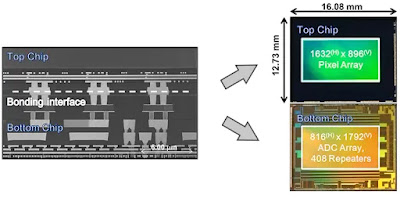
The inclusion of nearly 1,000 times as many ADCs compared to the traditional column-parallel ADC architecture means an increased demand for current. Sony addressed this issue by developing a compact 14-bit A/D converter which is said to boast the industry's best performance in low-current operation. The FoM of the new ADC is 0.24e-・nJ/step. (power consumption x noise) / {no. of pixels x frame speed x 2^(ADC resolution)}.
The connection between each pixel on the top chip uses Cu-Cu connection, that Sony put into mass production as a world-first in January 2016.
Main Features:
- Low-current, compact pixel-parallel A/D converter
In order to curtail power consumption, the new converter uses comparators that operate with subthreshold currents, resulting in the low current, compact 14-bit ADC. This overcomes the issue of the increased demand for current due to the inclusion of nearly 1,000 times as many ADCs in comparison with the traditional column ADC. - Cu-Cu (copper-copper) connection
To achieve the parallel A/D conversion for all pixels, Sony has developed a technology which makes it possible to include approximately three million Cu-Cu (copper-copper) connections in one sensor. The Cu-Cu connection provides electrical continuity between the pixel and logic substrate, while securing space for implementing as many as 1.46 million A/D converters, the same number as the effective megapixels, as well as the digital memory. - High-speed data transfer construction
Sony has developed a new readout circuit to support the massively parallel digital signal transfer required in the A/D conversion process using 1.46 million A/D converters, making it possible to read and write all the pixel signals at high speed.


They should have targeted 1080p resolution, pixel pitch might have been a little too big to fit I guess.
ReplyDeleteNo doubt limited by the copper to copper connections possible. This is the future though and once they start scaling this down the resolutions will get better and better and storage node global shutters will be a thing of the past. Eventually they'll do away with mechanical shutters as well on larger sensor cameras. Exciting times.
ReplyDeletehow about the FPN of this design?
ReplyDeletethis opens the road to event detectors as f.i. 'real time' single X-ray detection and integration. And exiting possibilities for detecting and imaging of manifolds of movements. Like the eye functions.
ReplyDeleteI recalled. I saw Sakakibara on isscc2012. He is going to destroy his previous work.
ReplyDelete